Loading video…


 17 Concepts
 138.5K views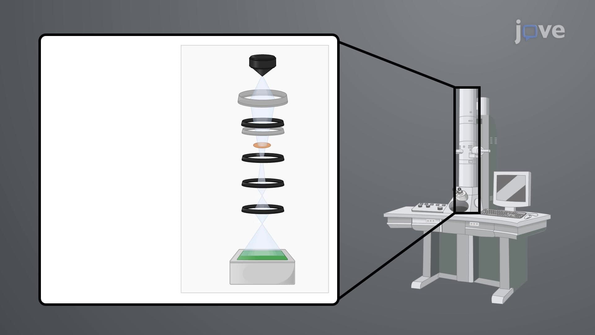

Video Summary: What Is Overview of Electron Microscopy
Did you know that researchers at Johns Hopkins University can see individual atoms using electron microscopy? An overview of electron microscopy reveals how these powerful instruments use electron beams instead of light to achieve magnifications up to 50 million times-far beyond what light microscopes can provide. Unlike traditional microscopes that max out at 2,000x magnification, electron microscopes create detailed images by directing focused electron beams through or across specimens in a vacuum environment. Watch the full video on JoVE Coach to master this concept with expert-led visuals and step-by-step explanations.
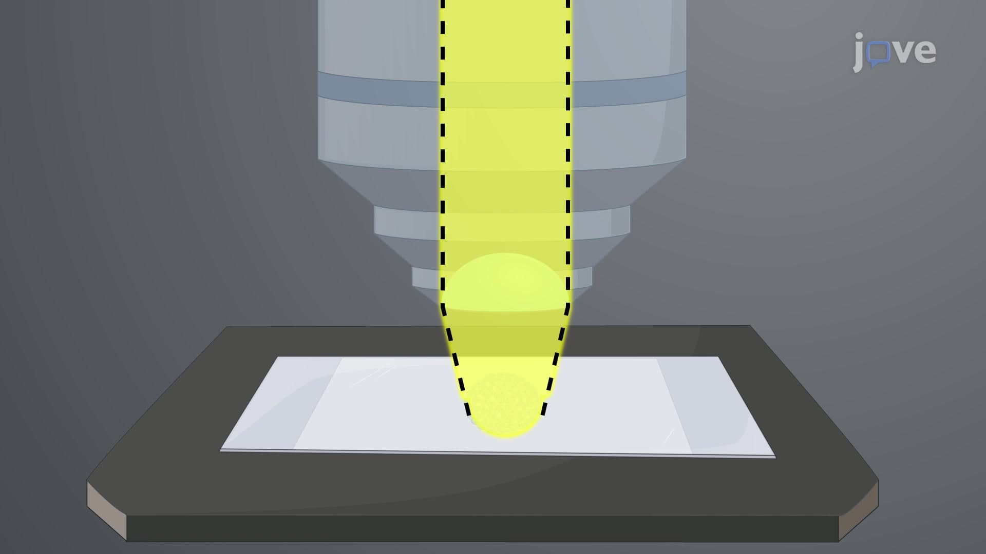
An overview of electron microscopy begins with recognizing why traditional light microscopy hits physical limitations. When high school students study cell biology or college undergraduates examine materials science, they quickly discover that light microscopes cannot resolve structures smaller than half the wavelength of visible light-roughly 200 nanometers. This limitation sparked the development of electron microscopy in the 1930s, revolutionizing scientific research across disciplines.
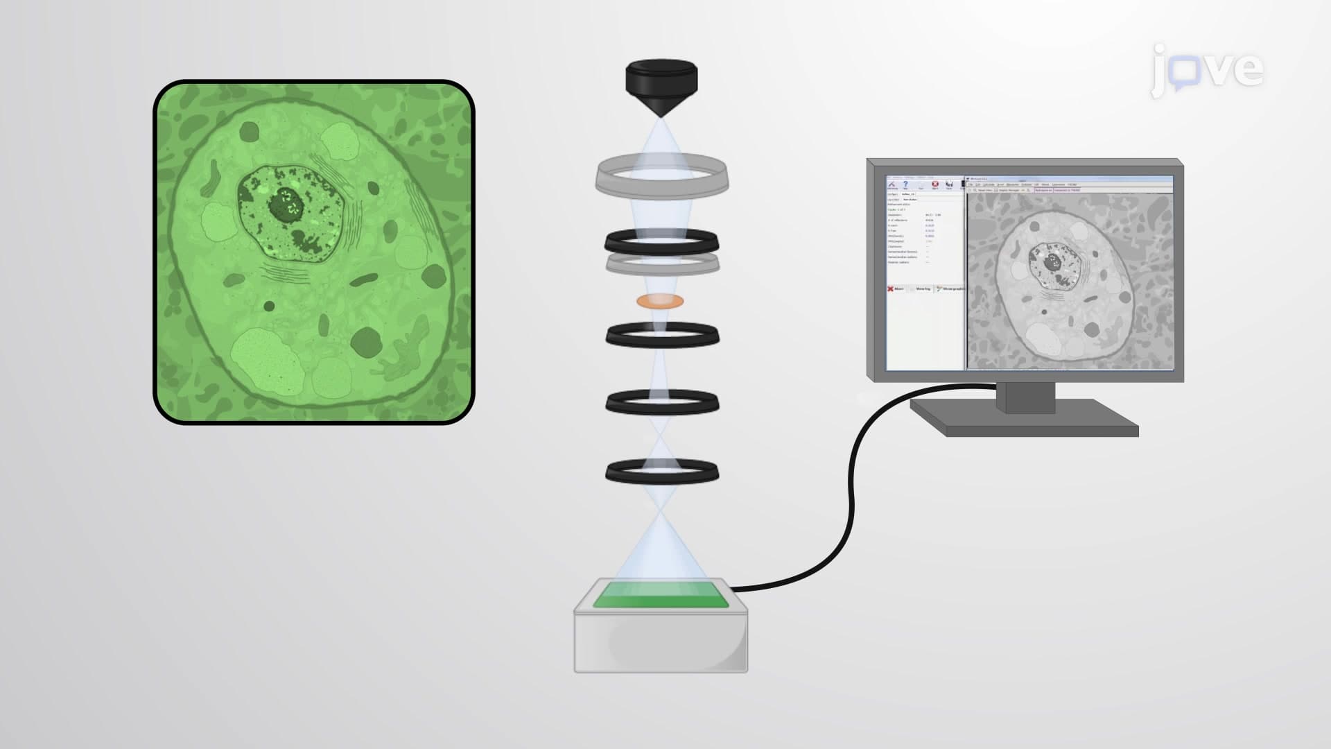
The heart of any electron microscope lies in its electron-emitting filament, typically made of tungsten or lanthanum hexaboride. This component generates a stream of electrons that travels through a sophisticated lens system. Unlike glass lenses in light microscopes, electron microscopes use electromagnetic and electrostatic lenses to manipulate the electron beam's path. Students preparing for AP Biology or college-level physics courses should understand that these "lenses" are actually magnetic fields that bend electron trajectories, similar to how a prism bends light.
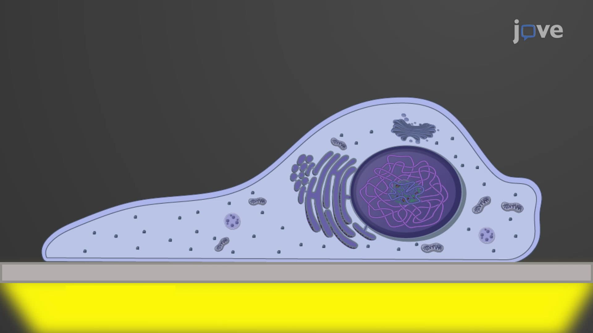
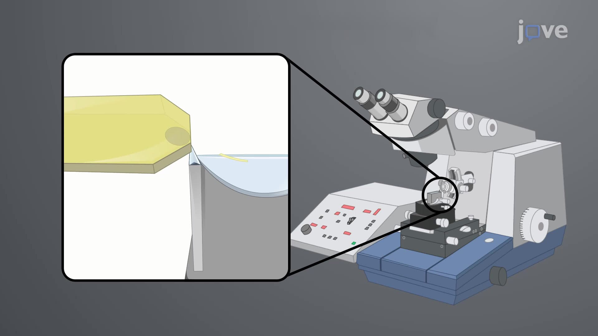
TEM operates by transmitting electrons through ultra-thin specimens, creating detailed 2D images of internal structures. At Stanford University's Materials Science department, researchers use TEM to analyze semiconductor defects crucial for Silicon Valley's technology industry. For students taking the MCAT, understanding TEM's ability to reveal organelle ultrastructure-such as mitochondrial cristae or endoplasmic reticulum detail-proves essential for cellular biology questions.
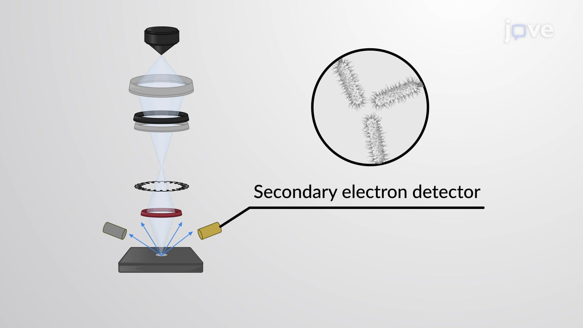
SEM takes a different approach, scanning electron beams across specimen surfaces and collecting reflected electrons to generate 3D-like images. The FDA regularly uses SEM to examine medical device surfaces, ensuring implant safety standards. College students studying materials engineering learn that SEM's ability to reveal surface topography at nanometer scales makes it invaluable for quality control in manufacturing processes from automotive components to pharmaceutical tablets.
This microscopy overview demonstrates how electron beam technology transformed scientific observation, enabling discoveries from virus structure identification to advanced materials characterization that drives American innovation in biotechnology and engineering sectors.
Related Micro-courses