Loading video…


 17 Concepts
 138.5K views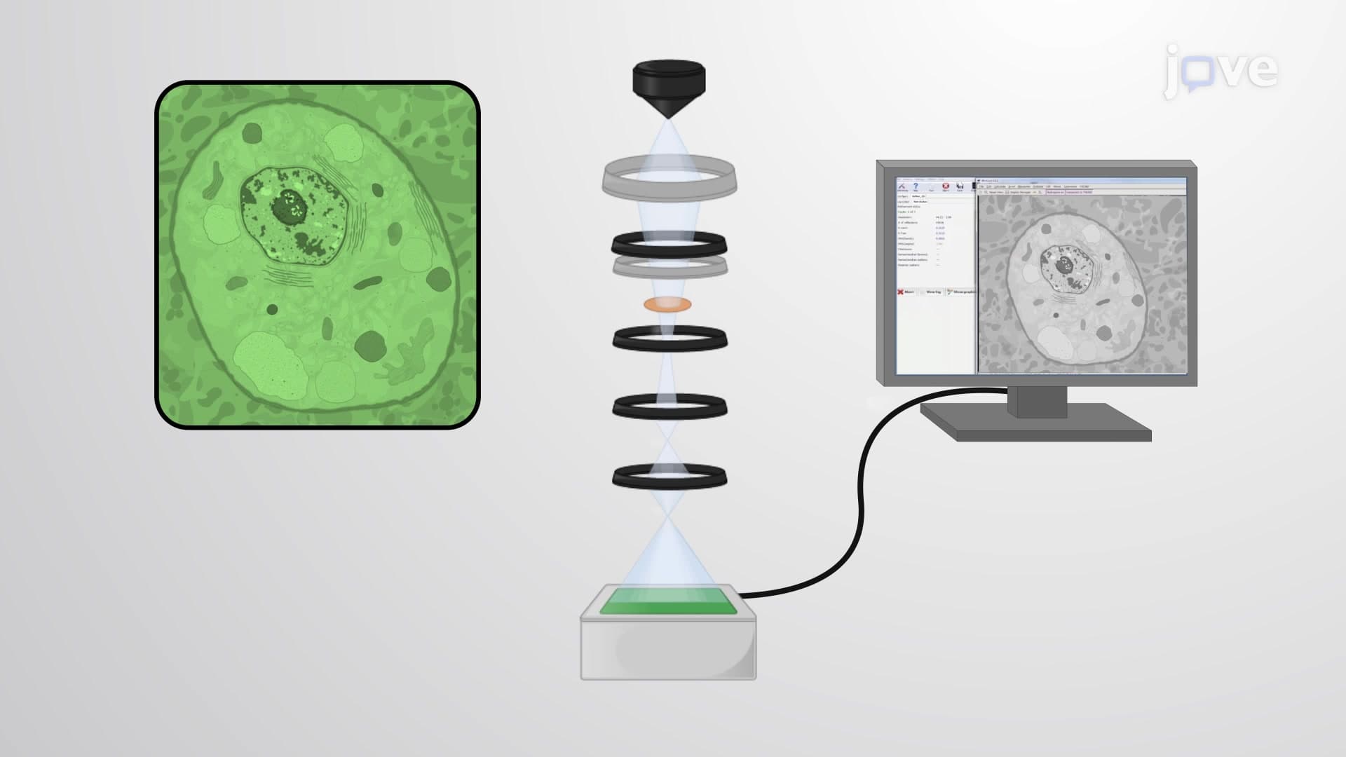

Video Summary: What Is Transmission Electron Microscopy
Did you know scientists can see structures 1,000 times smaller than what light microscopes reveal? Transmission electron microscopy uses high-energy electron beams instead of light to create incredibly detailed images of a sample's internal structure. For example, researchers at Stanford University use this technique to examine the atomic structure of semiconductor materials for developing faster computer chips. What is Transmission Electron Microscopy becomes clear when you understand it's like having X-ray vision for the microscopic world. Watch the full video on JoVE Coach to master this concept with expert-led visuals and step-by-step explanations.
Transmission electron microscopy represents a revolutionary imaging technique that has transformed scientific research since its development in the 1930s. Unlike conventional light microscopy, which uses photons, TEM employs a focused beam of high-energy electrons to probe the internal structure of materials with extraordinary resolution-often reaching the atomic scale.
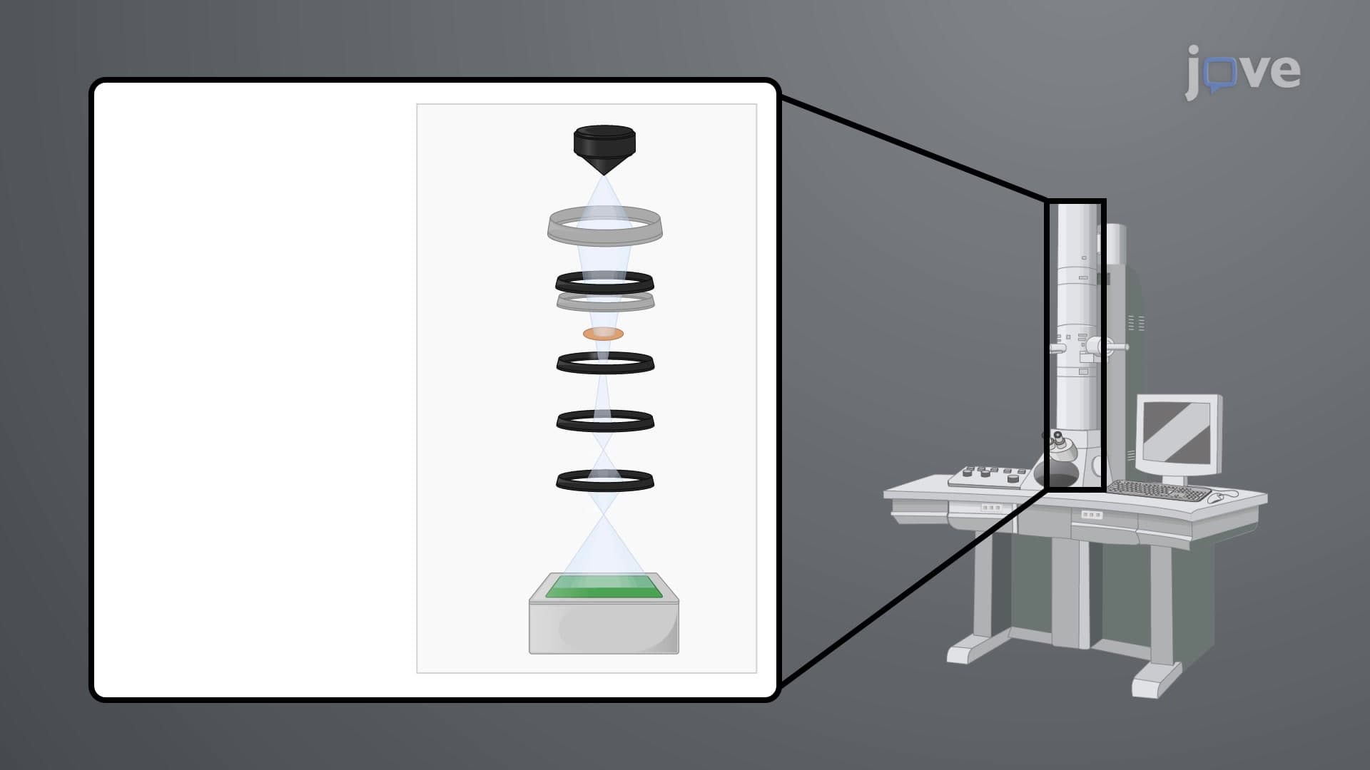
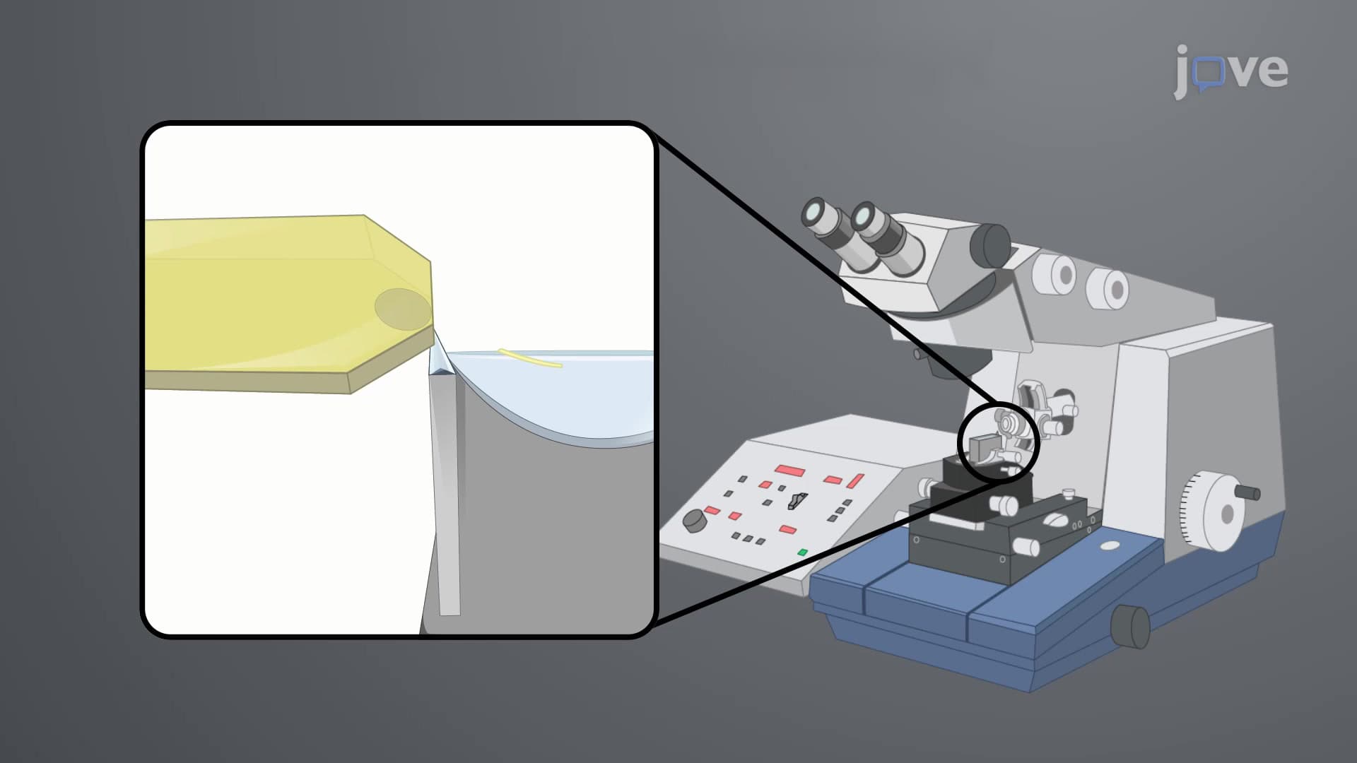
The transmission electron microscopy system operates through a sophisticated arrangement of electromagnetic components. An electron gun serves as the source, generating electrons that travel through a vacuum column. Multiple electromagnetic condenser lenses focus this electron beam onto an ultra-thin specimen, typically less than 100 nanometers thick. As electrons interact with the sample, some are scattered or absorbed while others pass through relatively unchanged.
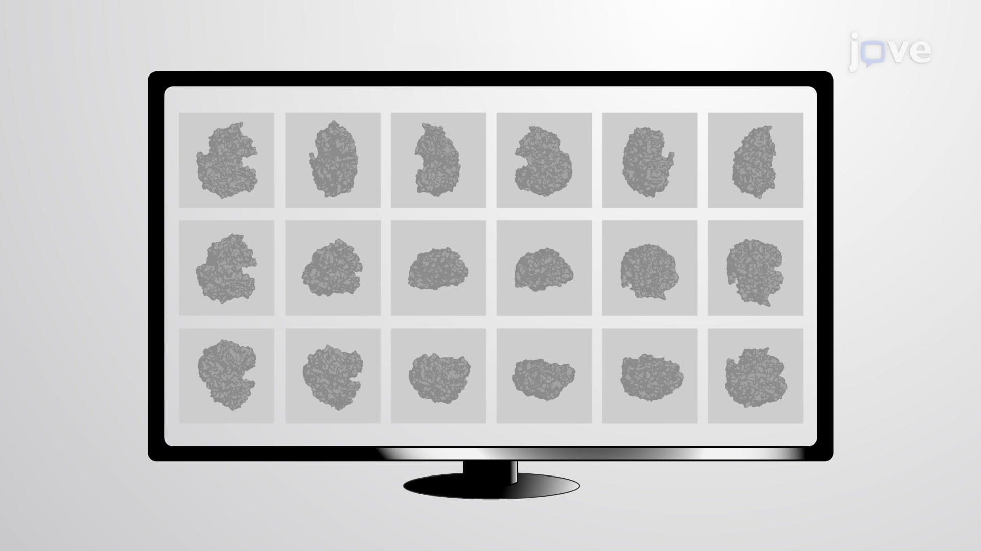
The transmitted electrons then encounter objective lenses, which form an initial magnified image. Additional intermediate and projector lenses further magnify this image, achieving total magnifications exceeding 1,000,000x. Modern TEM systems capture final images using digital CCD cameras or traditional phosphorescent screens, creating detailed two-dimensional representations of three-dimensional structures.
Transmission electron microscopy produces characteristic black and white images where contrast directly relates to sample density and thickness. Dense regions containing heavy atoms (like metals) appear darker because they scatter or absorb more electrons. Conversely, lighter areas indicate regions with lower atomic numbers or reduced thickness that allow greater electron transmission.
This contrast mechanism proves invaluable for studying biological specimens, where cellular organelles, membranes, and protein complexes exhibit different densities. For example, researchers at the National Institutes of Health use TEM to examine virus structures, helping develop vaccines and treatments.
Beyond imaging, transmission electron microscopy offers powerful analytical capabilities through electron energy-loss spectroscopy (EELS) and energy-dispersive X-ray spectroscopy (EDS). When high-energy electrons interact with sample atoms, they generate characteristic X-rays unique to each element. This enables precise elemental identification and quantification, making TEM essential for materials characterization in semiconductor manufacturing and nanotechnology research.
Students preparing for AP Chemistry or college-level materials science courses should understand how these analytical techniques complement structural imaging, providing comprehensive sample characterization crucial for research and industrial applications.
Related Micro-courses