Loading subject page…

- Cell Biology
- Visualizing Cells, Tissues, and Molecules
- Scanning Electron Microscopy
Micro-course: Visualizing Cells, Tissues, and Molecules
138,514 views
Learn key concepts and earn your certificate.








Scanning Electron Microscopy

00:00
01:07
Video Summary: What Is Scanning Electron Microscopy
Ever wondered how scientists can see details smaller than bacteria? Scanning electron microscopy revolutionizes our ability to visualize microscopic worlds invisible to traditional light microscopes. This powerful imaging technique uses focused electron beams to create detailed 3D surface images with magnifications reaching 500,000x. From analyzing semiconductor defects at Intel to examining blood cells at Mayo Clinic, what is scanning electron microscopy has become essential for breakthrough discoveries in materials science, biology, and nanotechnology research. Watch the full video on JoVE Coach to master this concept with expert-led visuals and step-by-step explanations.
- Understand what is scanning electron microscopy and how it differs from traditional light microscopy techniques
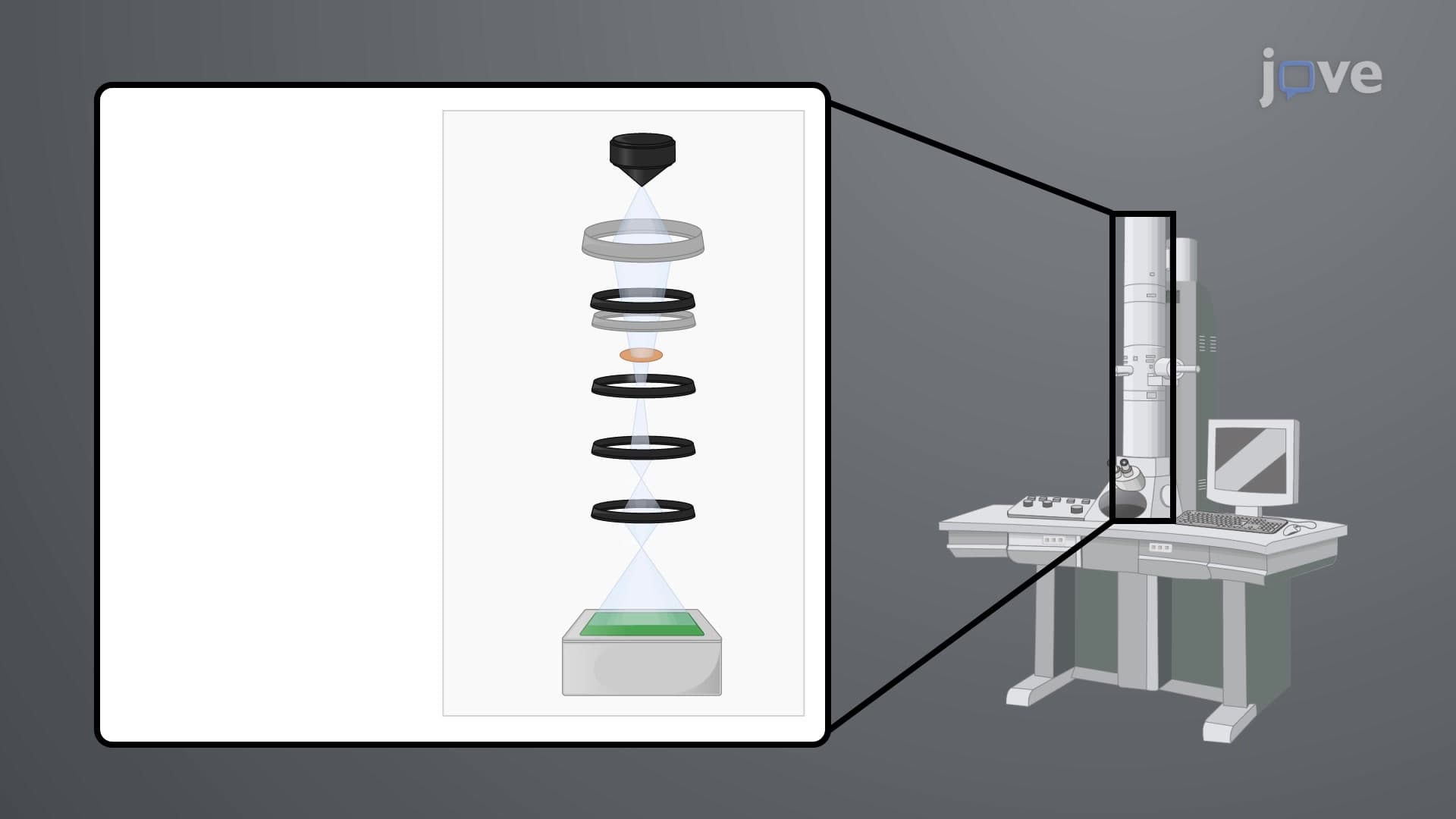
- Identify the key components of an SEM system, including the electron gun, electromagnetic lenses, and scanning coils
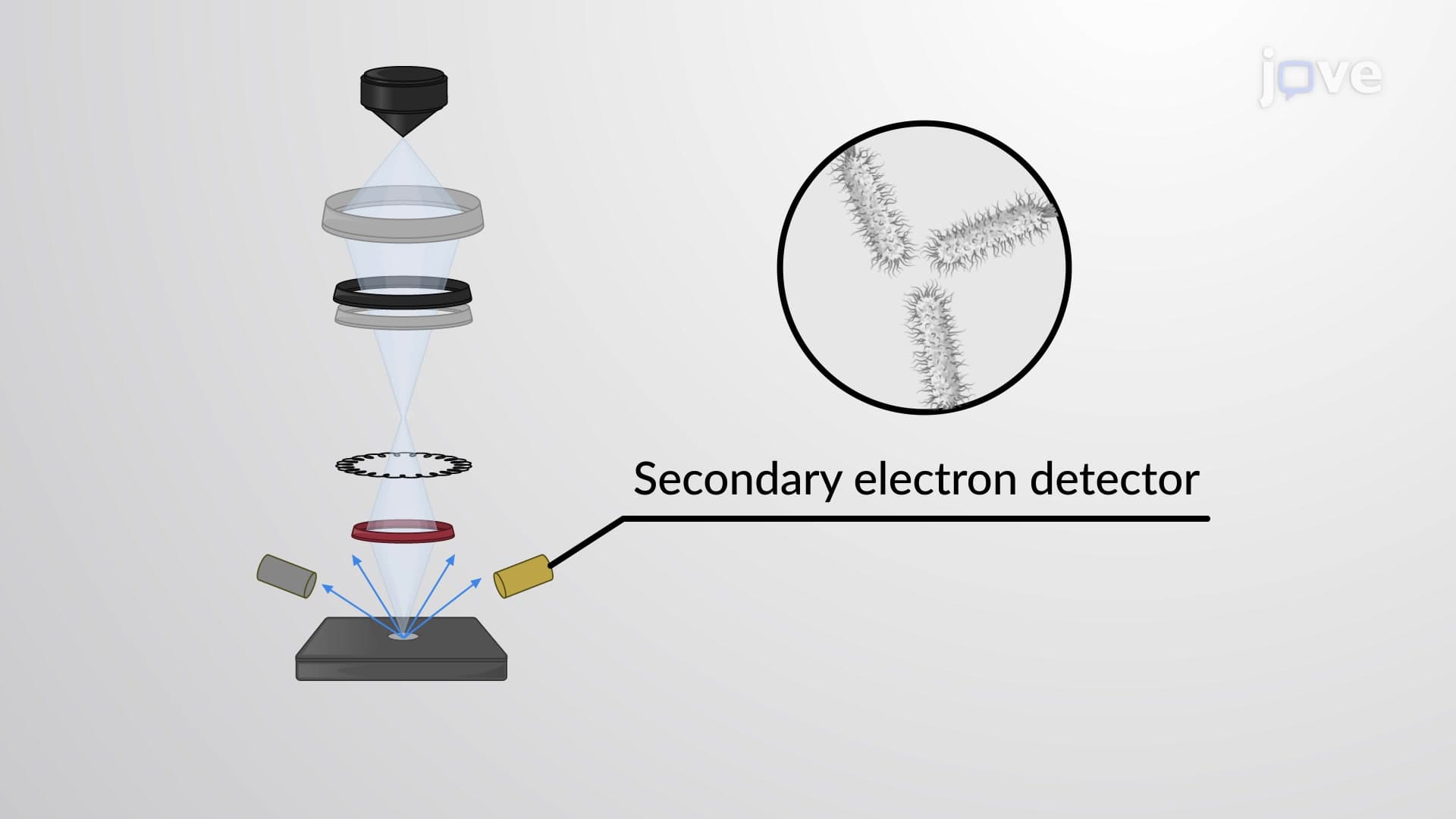
- Analyze how primary electron beams interact with sample surfaces to generate secondary electrons and characteristic X-rays
- Compare the advantages and limitations of scanning electron microscopy versus other imaging methods
- Evaluate the role of sample preparation in achieving high-quality SEM images
- Apply knowledge of electron-sample interactions to interpret SEM imaging results
- Recognize real-world applications of SEM technology in materials science, biology, and quality control
- Explore how electromagnetic lenses focus and control electron beam diameter for optimal resolution
What is Scanning Electron Microscopy: Core Principles
Scanning electron microscopy represents a quantum leap in imaging technology that has transformed scientific research since its commercial introduction in the 1960s. Unlike traditional light microscopes limited by wavelength constraints, SEM systems harness the wave-particle duality of electrons to achieve unprecedented resolution and magnification capabilities.
The fundamental scanning electron microscopy concept relies on electron-matter interactions rather than photon transmission. When a focused electron beam strikes a sample surface, it penetrates several micrometers deep, creating an interaction volume where various phenomena occur simultaneously. This interaction zone becomes the source of multiple signals that SEM systems detect and process into meaningful images.
Electron Beam Generation and Control Systems
The heart of any SEM system begins with the electron gun, typically a tungsten filament or field emission source that generates a stream of negatively charged electrons. These electrons accelerate toward a positively charged anode, gaining kinetic energy proportional to the applied voltage-usually ranging from 1,000 to 30,000 volts in modern instruments.
Electromagnetic lenses play a crucial role in this scanning electron microscopy overview by focusing the electron beam to diameters as small as 1-5 nanometers. These lenses operate similarly to optical lenses but use magnetic fields instead of curved glass surfaces. The condenser lens system reduces beam diameter while maintaining sufficient current for image formation, creating the optimal balance between resolution and signal strength.
Signal Detection and Image Formation
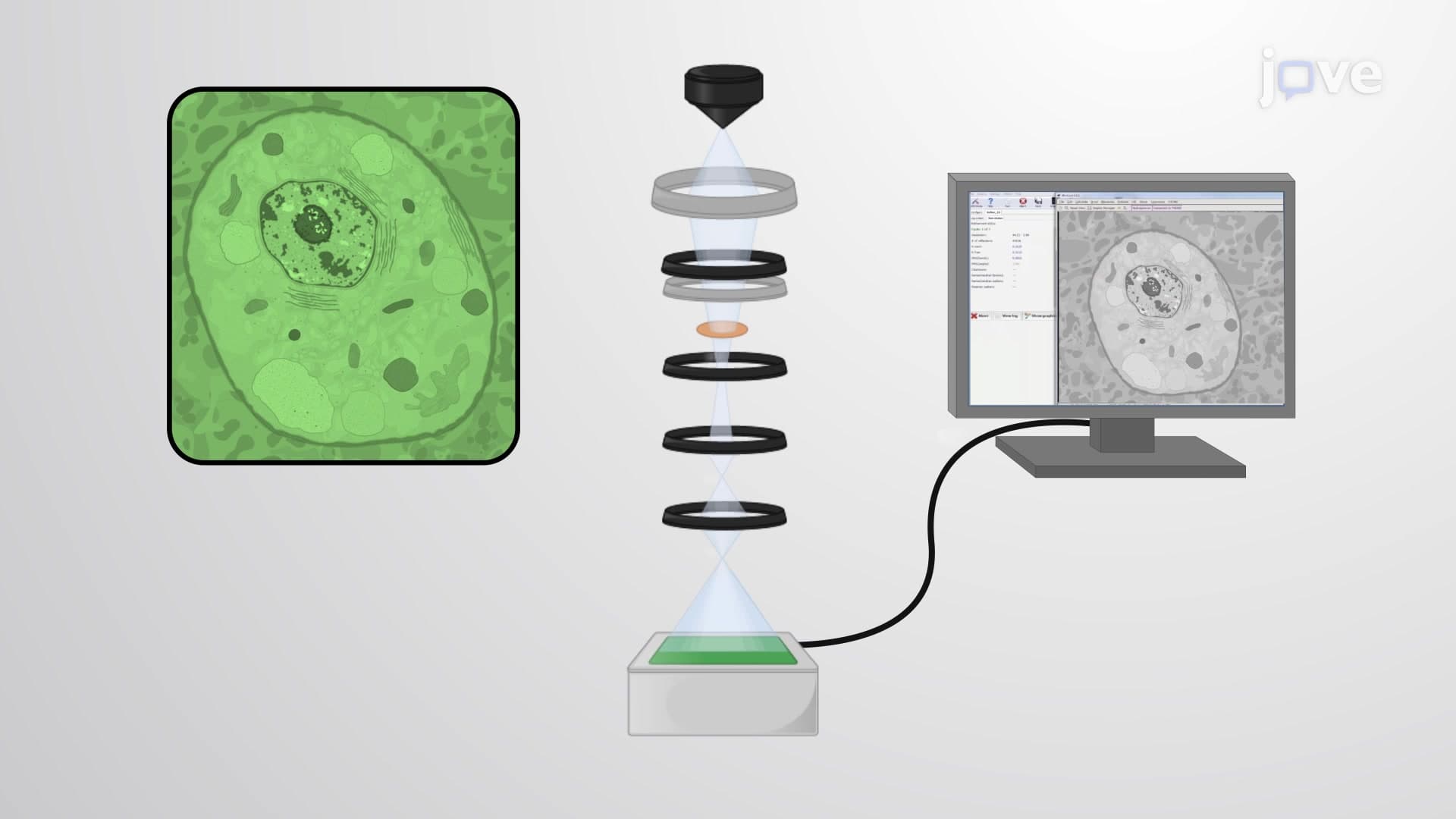
The scanning electron microscopy basics involve understanding how secondary electrons create the final image. When primary electrons from the beam interact with sample atoms, they transfer energy that ejects loosely bound secondary electrons from the specimen surface. These secondary electrons, typically having energies below 50 electron volts, provide topographical information about the sample.
Simultaneously, characteristic X-rays emerge from deeper within the sample when primary electrons displace inner-shell electrons from sample atoms. Each element produces a unique X-ray signature, enabling elemental analysis and compositional mapping-a technique particularly valuable in metallurgy and semiconductor manufacturing.
Applications in Academic and Professional Settings
Understanding scanning electron microscopy proves essential for students pursuing STEM careers. AP Biology students encounter SEM images when studying cell ultrastructure, while AP Chemistry courses reference SEM analysis of crystal structures and surface catalysis. College-level materials science programs extensively use SEM data interpretation, making this knowledge crucial for engineering majors.
Professional applications span from NASA's analysis of space dust particles to pharmaceutical companies examining drug delivery mechanisms. Major US research institutions like MIT, Stanford, and the National Institute of Standards and Technology rely heavily on SEM technology for breakthrough discoveries in nanotechnology, biomedicine, and advanced materials development.
Frequently Asked Questions
Scanning electron microscopy is an imaging technique that uses a focused electron beam to scan sample surfaces and create highly detailed 3D images. The electron beam interacts with sample atoms, producing secondary electrons and X-rays that detectors convert into visual information. This process achieves magnifications up to 500,000x with resolution down to 1-5 nanometers, far exceeding traditional light microscopy capabilities.
MCAT passages often include SEM images in experimental contexts, requiring students to interpret electron micrographs and understand resolution limitations. AP Biology exams feature SEM images of cellular structures, while college chemistry exams test understanding of electron-sample interactions. Students should focus on comparing SEM capabilities with light microscopy and recognizing typical SEM image characteristics.
SEM technology drives innovation across multiple industries, from semiconductor manufacturing at companies like Intel and AMD to medical device development at Medtronic and Johnson & Johnson. Universities use SEM for materials characterization, while government labs like Sandia National Laboratories employ it for national security research. This versatility makes SEM knowledge valuable for students entering diverse STEM fields.
High school physics knowledge provides sufficient foundation for understanding basic SEM principles. Key prerequisites include electromagnetic concepts, atomic structure, and wave-particle duality-topics covered in AP Physics and introductory college courses. The mathematical complexity remains manageable, focusing more on conceptual understanding than complex calculations, making it accessible to motivated students.
Create comparison charts highlighting differences between SEM, TEM (transmission electron microscopy), and light microscopy regarding resolution, sample preparation, and applications. Practice interpreting SEM images from textbooks and research papers, focusing on identifying surface features and understanding magnification scales. Memorize key specifications like typical accelerating voltages (1-30 kV) and resolution limits.
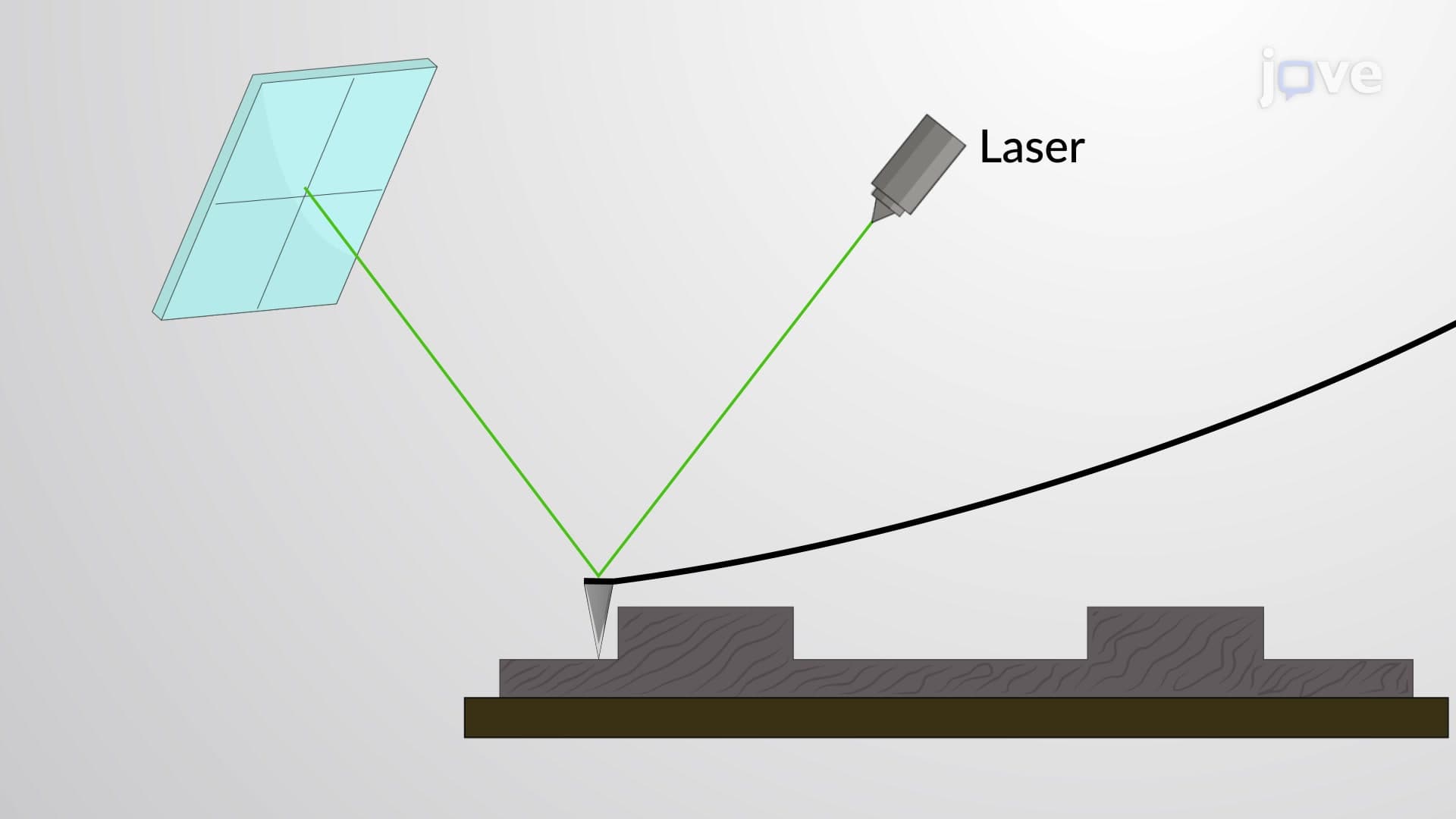
SEM serves as a gateway to understanding other electron microscopy methods like transmission electron microscopy (TEM) and atomic force microscopy (AFM). These complementary techniques share fundamental principles while offering different capabilities-TEM for internal structure analysis and AFM for surface topography mapping. Mastering SEM concepts provides excellent preparation for advanced materials characterization courses.
SEM skills open doors to research positions at national laboratories, semiconductor companies, pharmaceutical firms, and academic institutions. Materials scientists, biomedical engineers, forensic analysts, and quality control specialists regularly use SEM technology. Graduate programs in engineering, materials science, and applied physics highly value students with hands-on SEM experience from undergraduate research projects.
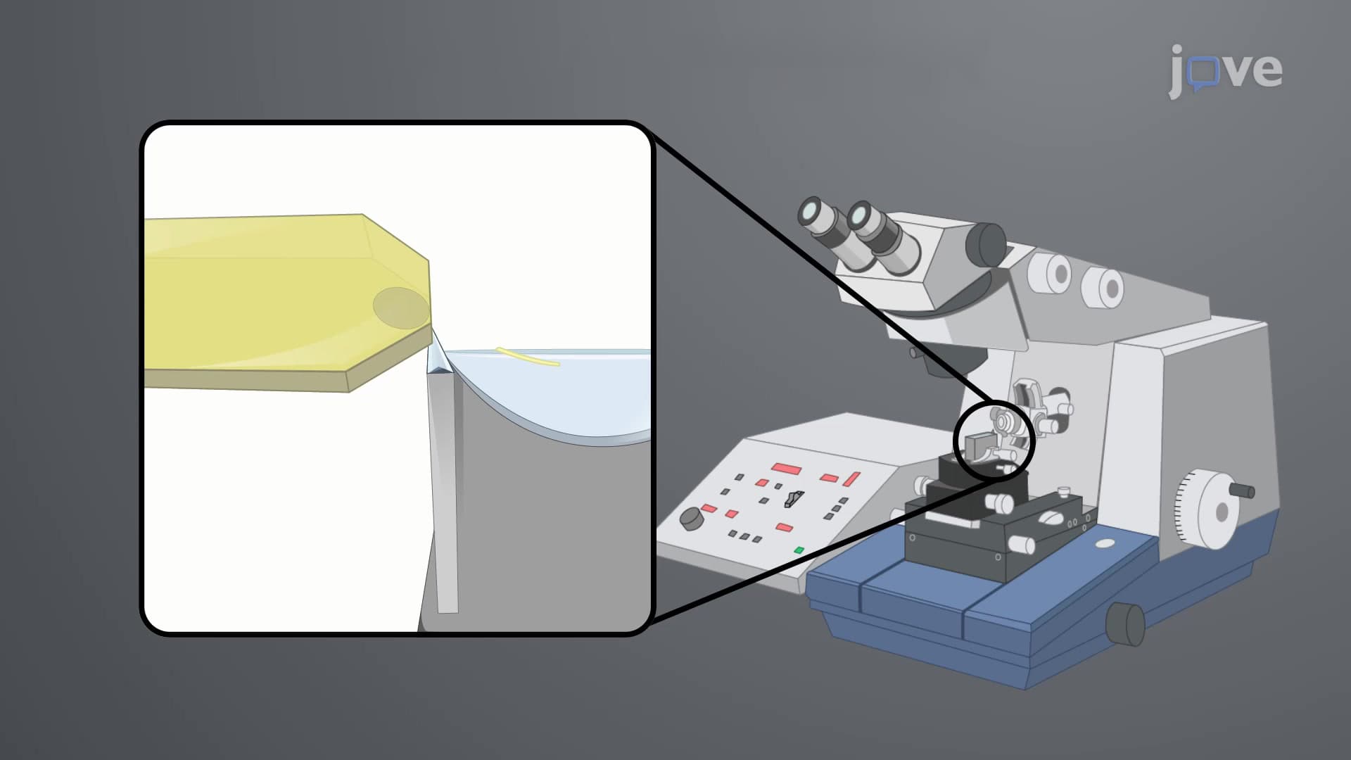
Biological samples require dehydration and conductive coating to prevent charging effects, while metals need careful polishing to reveal microstructures. Non-conductive materials must be coated with thin gold or carbon films to enable electron flow. Understanding these preparation requirements helps students appreciate why SEM sample prep often determines image quality more than instrument settings, a concept frequently tested in laboratory courses.
Related Micro-courses