Loading…
Loading video…

16,136 views
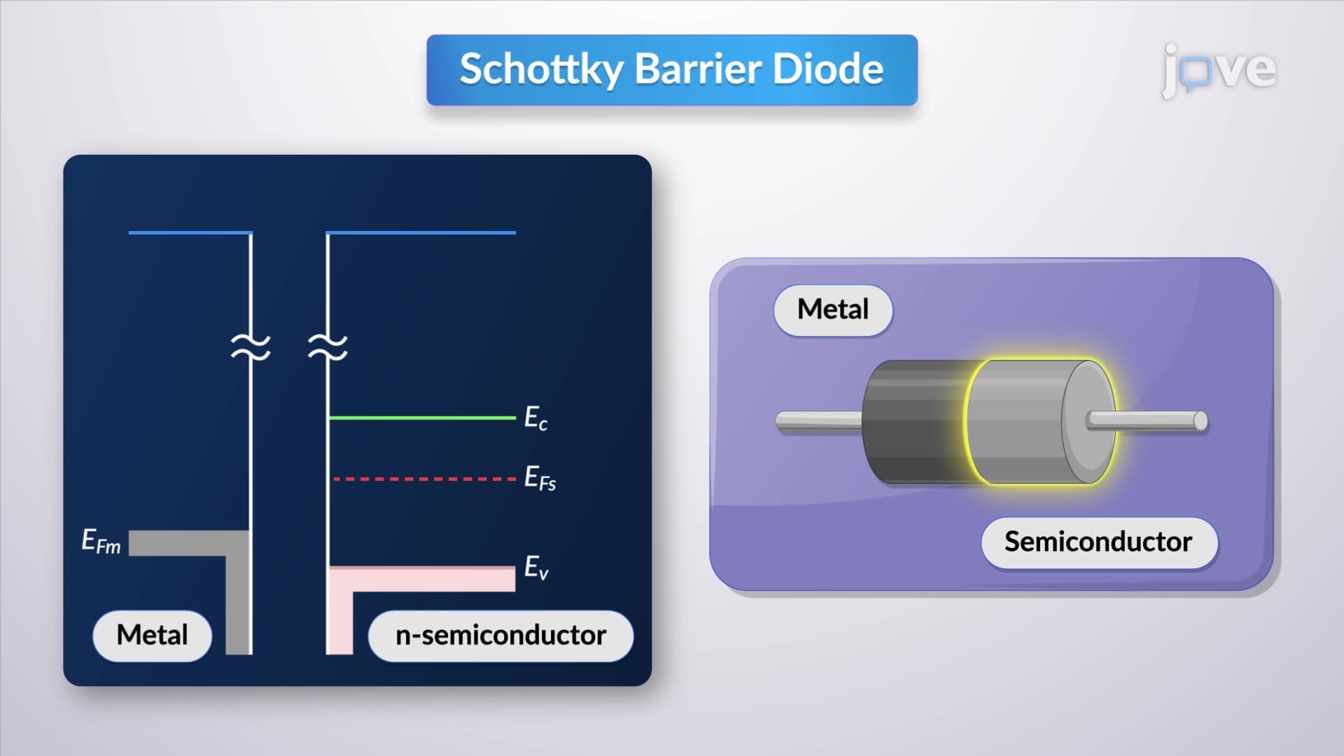
Did you know that the high-voltage power supplies in older CRT televisions and computer monitors rely on voltage doubler circuits to transform standard household electricity into the thousands of volts needed for display operation? A schottky barrier diode plays a crucial role in modern voltage doubler implementations due to its fast switching characteristics. These circuits, including the voltage doubler circuit configuration, are essential components in American-made medical equipment like portable defibrillators and X-ray machines. Watch the full video on JoVE Coach to master this concept with expert-led visuals and step-by-step explanations.
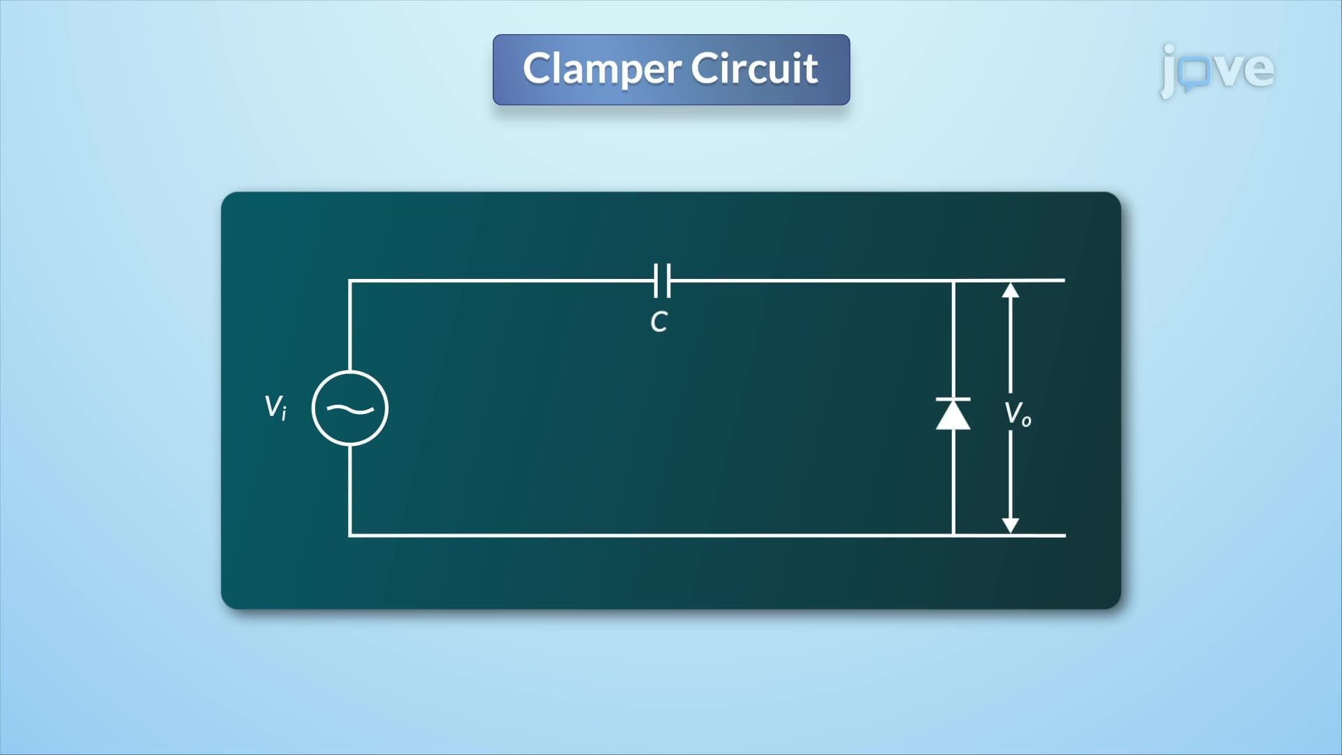
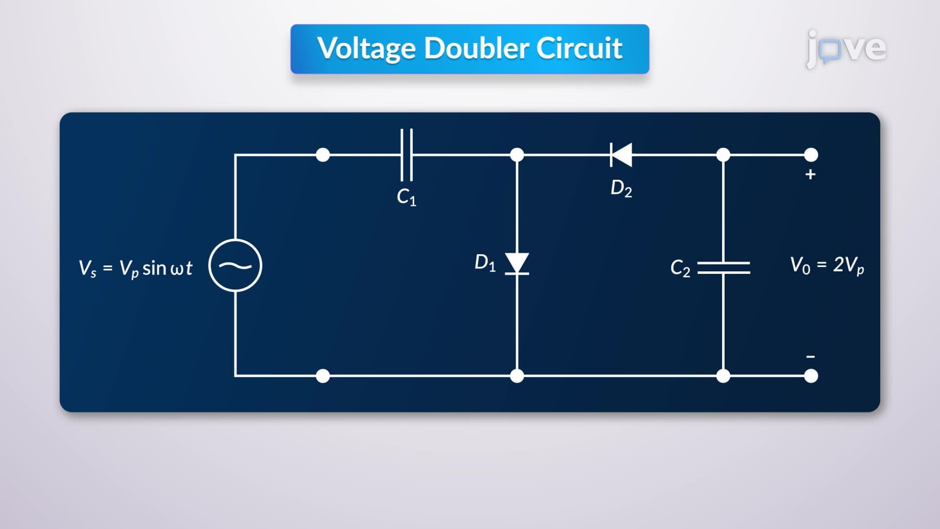
A voltage doubler circuit represents one of the most elegant solutions in power electronics for achieving voltage multiplication without transformers. This circuit topology consists of two distinct functional blocks: a clamping section and a rectifier section, working in tandem to produce a DC output voltage that is twice the peak amplitude of the AC input signal.
The clamping section, comprising capacitor C1 and diode D1, performs a critical voltage shifting function. When a sinusoidal input is applied, this section clamps the positive voltage peaks to zero while allowing negative peaks to reach twice the input amplitude. This creates a shifted waveform that serves as the input to the rectifier section. The schottky barrier diode definition becomes particularly relevant here, as these devices offer superior switching characteristics compared to conventional PN junction diodes, reducing voltage drops and improving overall circuit efficiency.
The rectifier section, containing diode D2 and capacitor C2, then converts this shifted AC waveform into a stable DC voltage. The final output voltage equals twice the peak value of the original sinusoidal input, hence the "voltage doubler" designation. Students preparing for AP Physics C or introductory electrical engineering courses at universities like MIT or Stanford will encounter this principle as a fundamental example of capacitive voltage multiplication.
Understanding what is schottky barrier diode in detail becomes crucial when examining modern voltage doubler implementations. These specialized diodes, featuring a metal-semiconductor junction rather than a PN junction, provide faster switching speeds and lower forward voltage drops. This makes them ideal for high-frequency switching applications found in switch-mode power supplies used in laptops, smartphones, and LED drivers manufactured by companies like Texas Instruments and Analog Devices.
Voltage doublers find extensive use in medical equipment, particularly in portable defibrillators used by emergency medical services across the United States. They're also essential in scientific instrumentation, including photomultiplier tube power supplies used in research facilities at institutions like the National Institute of Standards and Technology (NIST). For college students taking circuits courses, voltage doublers appear frequently in ABET-accredited electrical engineering programs as examples of practical circuit design principles that bridge theoretical knowledge with real-world applications.
Frequently Asked Questions
A voltage doubler circuit is an electronic configuration that produces a DC output voltage twice the peak amplitude of its AC input. It uses two stages: a clamping section that shifts the input waveform, and a rectifier section that converts the shifted signal to DC, effectively doubling the voltage without requiring transformers.
Schottky barrier diodes enhance voltage doubler circuits through faster switching speeds and lower forward voltage drops compared to standard silicon diodes. Their metal-semiconductor junction design reduces power losses and improves efficiency, making them ideal for high-frequency applications in modern power supplies and DC-DC converters.
Yes, voltage doublers frequently appear on AP Physics C Electricity and Magnetism exams and introductory electrical engineering courses at ABET-accredited programs. Students should understand circuit operation, waveform analysis, and be able to calculate output voltages given specific input parameters for both multiple-choice and free-response questions.
Voltage doublers are extensively used in American-manufactured medical equipment like portable defibrillators, CRT displays in older televisions and oscilloscopes, photomultiplier tube power supplies in research laboratories, and DC-DC converters in consumer electronics including laptop chargers and LED lighting systems.
No, voltage doublers require only basic algebra and trigonometry typically covered in high school physics. Understanding sine wave properties, capacitor charging/discharging, and diode behavior is sufficient. The concept builds naturally from fundamental circuit analysis principles taught in introductory physics and electrical engineering courses.
Focus on drawing and analyzing waveforms at each circuit stage, practice calculating output voltages from given input parameters, and understand how component values affect performance. Create step-by-step circuit operation sequences and work through numerical problems from textbooks like those used in MIT's 6.002 or Stanford's EE101 courses.
Voltage doublers can be cascaded or modified to create voltage triplers, quadruplers, and higher multiplication circuits. These extensions use additional diode-capacitor stages following the same clamping and rectification principles, making them valuable for applications requiring very high DC voltages from low-voltage AC sources.
Progress to more complex power electronics topics including switch-mode power supplies, voltage regulators, and DC-DC converter topologies like buck and boost converters. These advanced topics build directly on voltage doubler principles and are essential for electrical engineering students pursuing power systems or electronics design careers.
Related Micro-courses


Related Subjects
 Civil Engineering 30 micro-courses›Mechanical Engineering 28 micro-courses›