Loading video…


 12 Concepts
 46.1K views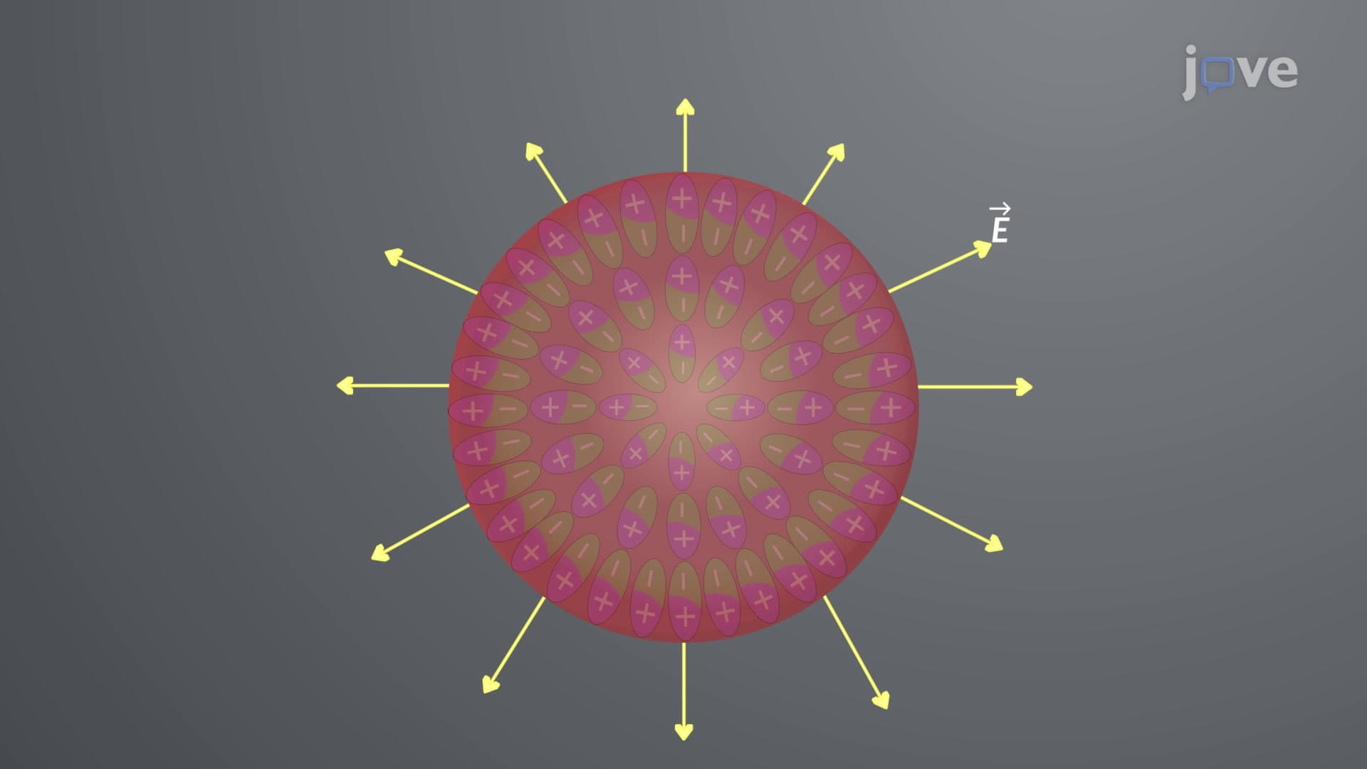

Video Summary: Potential Due to a Polarized Object Explained
Ever wondered how your smartphone's capacitive touchscreen detects your finger without physical contact? The potential due to a polarized object explains this phenomenon through electric field interactions with dielectric materials. When polarized materials create bound charges at surfaces and within volumes, they generate electric potentials that modern devices exploit. From medical imaging equipment at Johns Hopkins Hospital to semiconductor manufacturing in Silicon Valley, understanding how polarized dielectrics create electric potential fields is fundamental to countless technologies. Watch the full video on JoVE Coach to master this concept with expert-led visuals and step-by-step explanations.
When dielectric materials encounter external electric fields, they don't just passively respond-they actively reshape the field through polarization. This potential due to a polarized object represents one of electromagnetism's most practically important phenomena, governing everything from capacitor design to medical imaging technology.
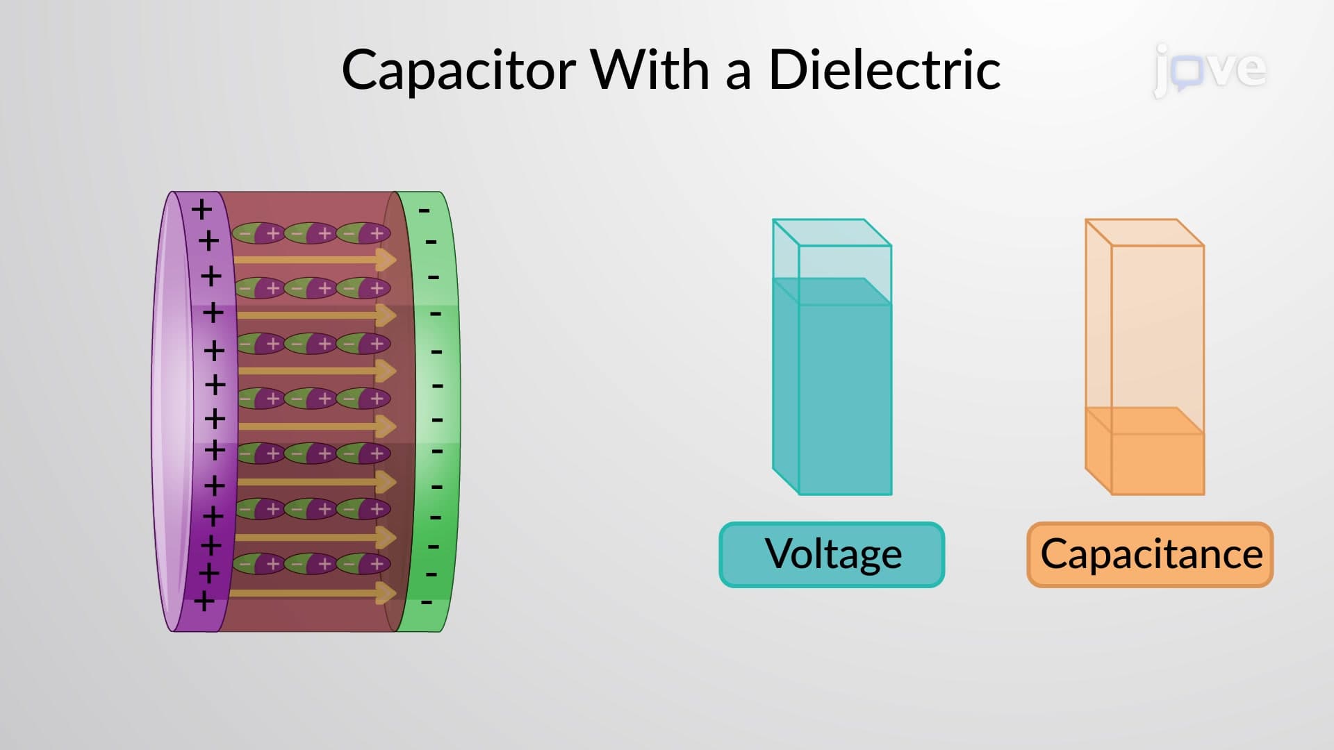
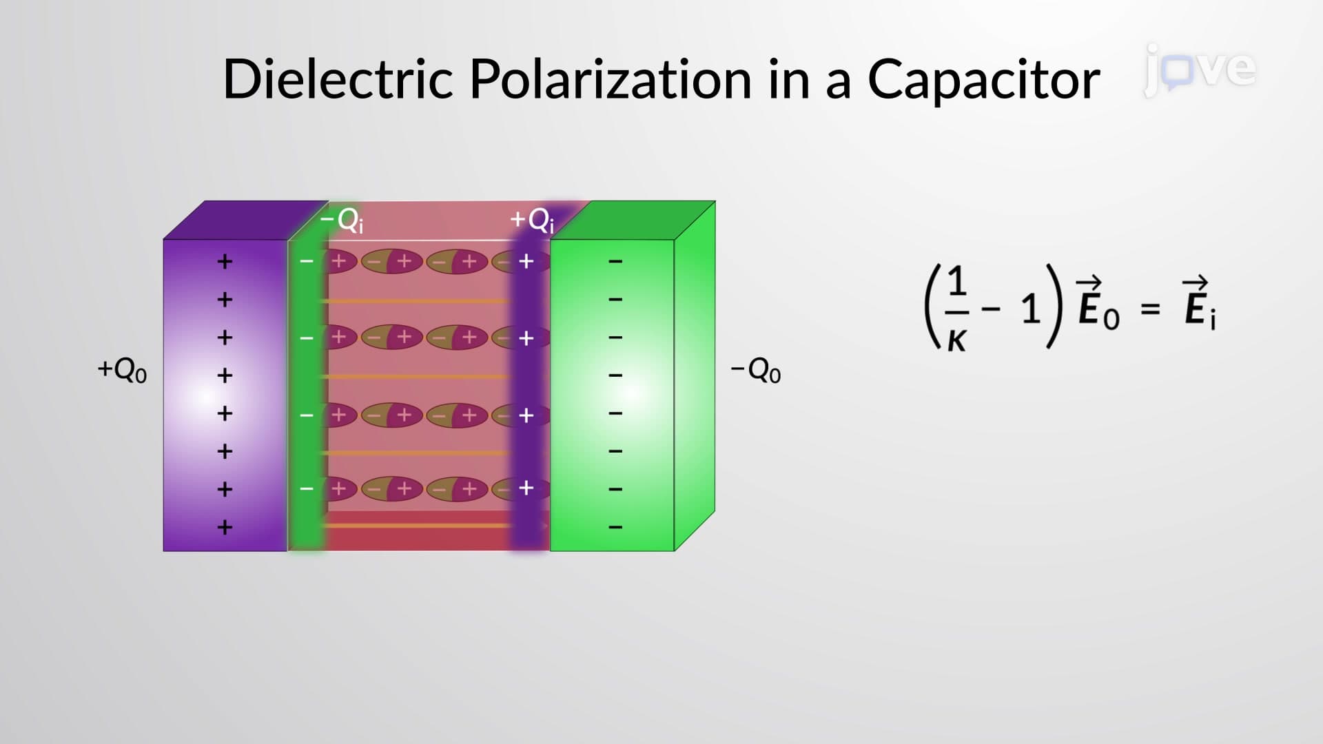
The polarization process creates fascinating charge distributions. Imagine a dielectric slab placed between parallel plates in a laboratory capacitor at MIT's physics department. As dipoles align with the external field, adjacent dipoles effectively cancel each other's charges internally, but at the surfaces, uncompensated charges accumulate. These surface-bound charges create their own electric field and potential.
The surface-bound charge density σ(bound) relates directly to the polarization vector P through the relationship σ(bound) = P · n̂, where n̂ represents the outward normal to the surface. This mathematical elegance appears frequently on AP Physics C exams and college-level electromagnetism courses, making it essential for students pursuing STEM careers.
When polarization varies spatially-common in real-world applications like the dielectric materials in smartphone capacitors-volume-bound charges emerge. These charges satisfy ρ(bound) = -∇ · P, creating a complete picture of how polarized materials generate electric potentials.
Consider medical imaging equipment used at UCLA Medical Center. The varying dielectric properties of different tissues create non-uniform polarization patterns, generating volume-bound charges that contribute to the imaging contrast. Understanding these contributions helps biomedical engineers optimize imaging protocols.
The potential due to a polarized object follows superposition principles, combining contributions from both surface and volume distributions. For practical calculations-whether on MCAT physics sections or college midterm exams-students must recognize that V(total) = V(surface-bound) + V(volume-bound).
This approach proves invaluable in engineering applications. Semiconductor manufacturers in California's Silicon Valley rely on these principles when designing integrated circuits with multiple dielectric layers. Each layer contributes to the total potential field, affecting device performance and reliability.
The mathematical framework extends beyond academic exercises, forming the foundation for capacitor design, electromagnetic simulation software, and advanced materials research across American universities and technology companies.
Related Micro-courses