Loading video…


 11 Concepts
 9.9K views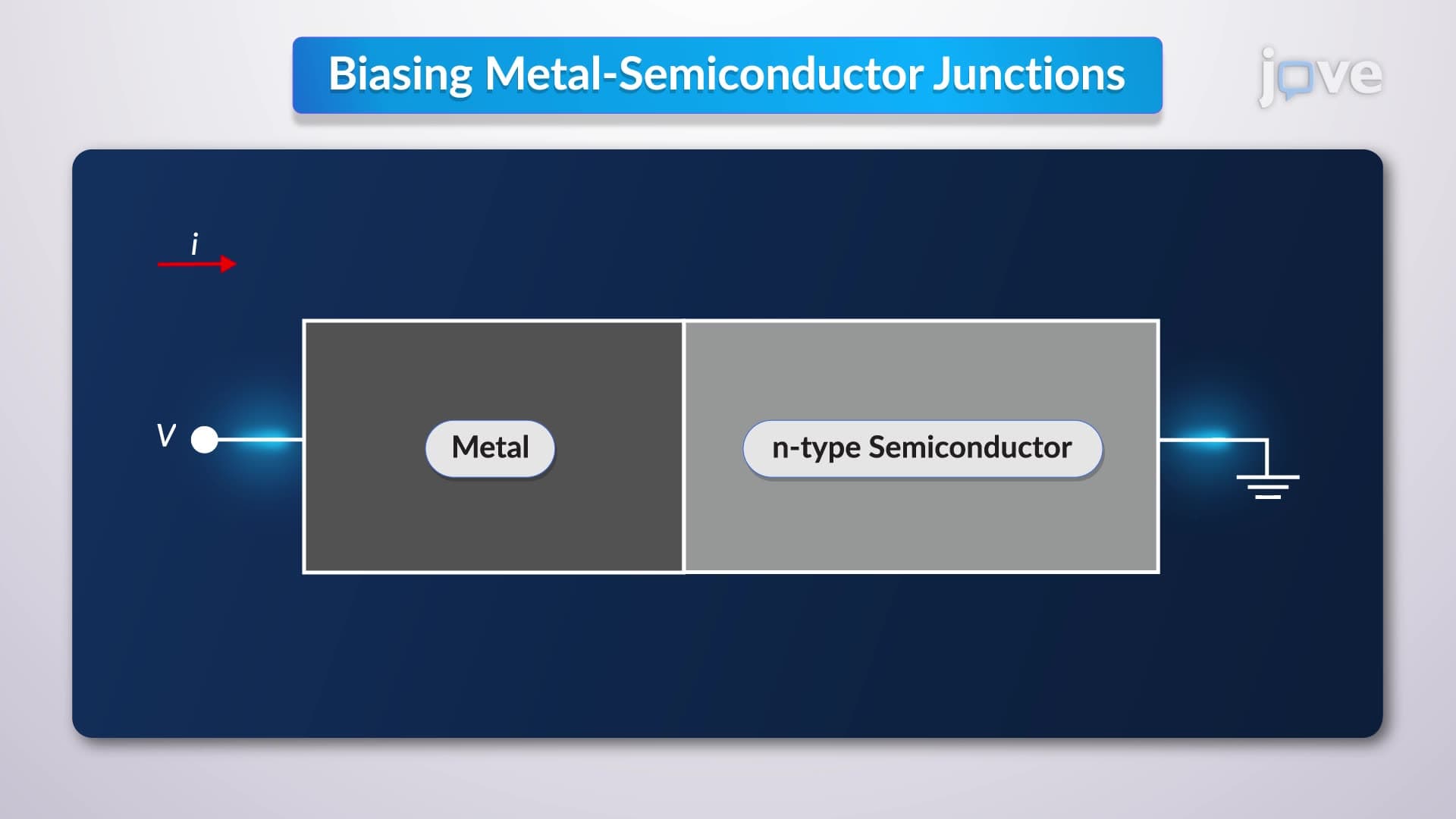

Video Summary: Biasing of Metal Semiconductor Junctions Explained
Ever wondered how your smartphone screen responds to touch or how solar panels convert sunlight into electricity? The Fermi level shifts dramatically when voltage is applied to metal-semiconductor junctions, creating the foundation for these everyday technologies. In Schottky diodes used in iPhone chargers, positive biasing lowers the metal's Fermi level, reducing electron barriers and enabling current flow from semiconductor to metal. Understanding biasing of metal semiconductor junctions explained reveals how engineers control electron movement in modern electronics. Watch the full video on JoVE Coach to master this concept with expert-led visuals and step-by-step explanations.
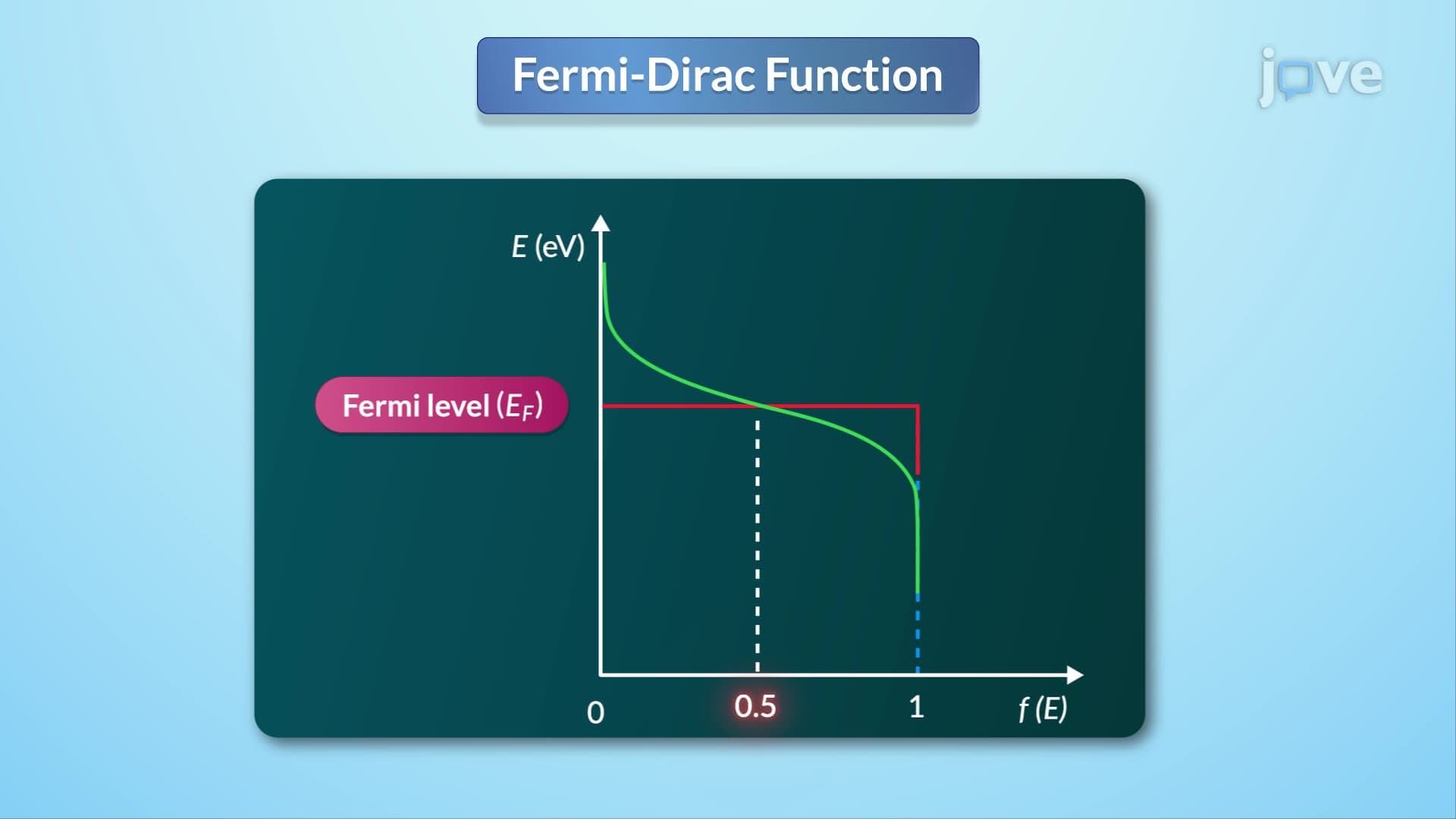
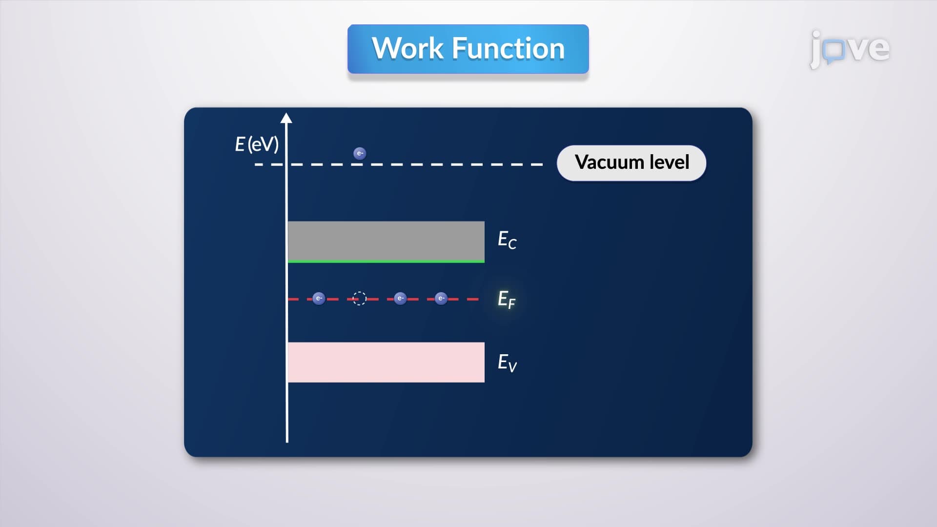
The Fermi level represents the highest energy level occupied by electrons at absolute zero temperature, serving as a crucial reference point for understanding electronic behavior in materials. When studying Fermi level definition, think of it as the "water level" in a container-electrons naturally flow from higher to lower Fermi levels, just like water flows downhill.
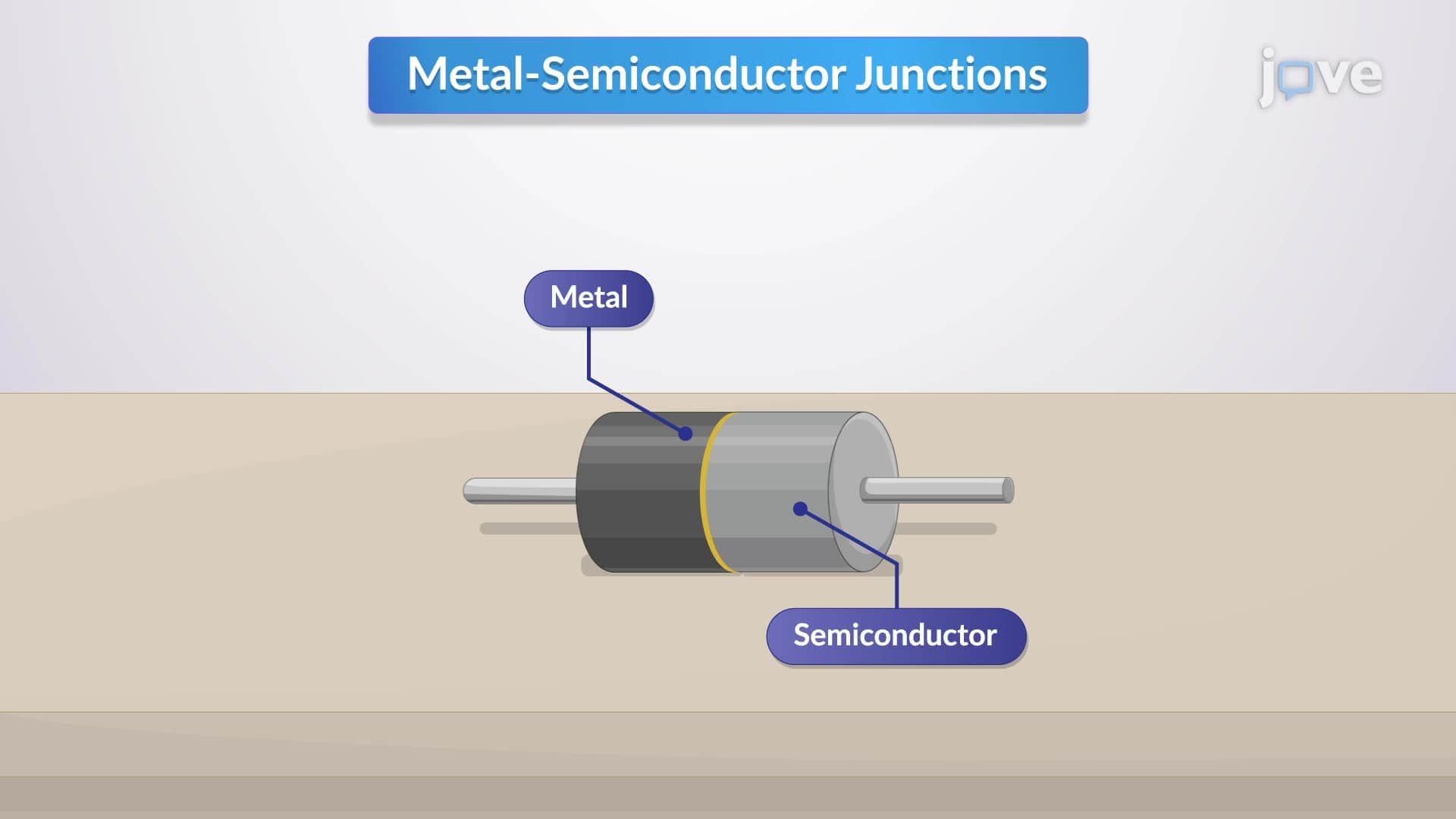
What is Fermi level in detail becomes clearer when examining energy band diagrams. In metals, the Fermi level lies within the conduction band, allowing free electron movement. In semiconductors, it typically sits in the bandgap between valence and conduction bands. When a metal contacts a semiconductor, their Fermi levels must align at thermal equilibrium, creating an energy barrier at the interface.
This Fermi level concept proves essential for AP Physics students and college engineering majors studying solid-state electronics. The barrier height depends on the work function difference between materials-a key topic in MCAT Physical Sciences sections covering electronic structure.
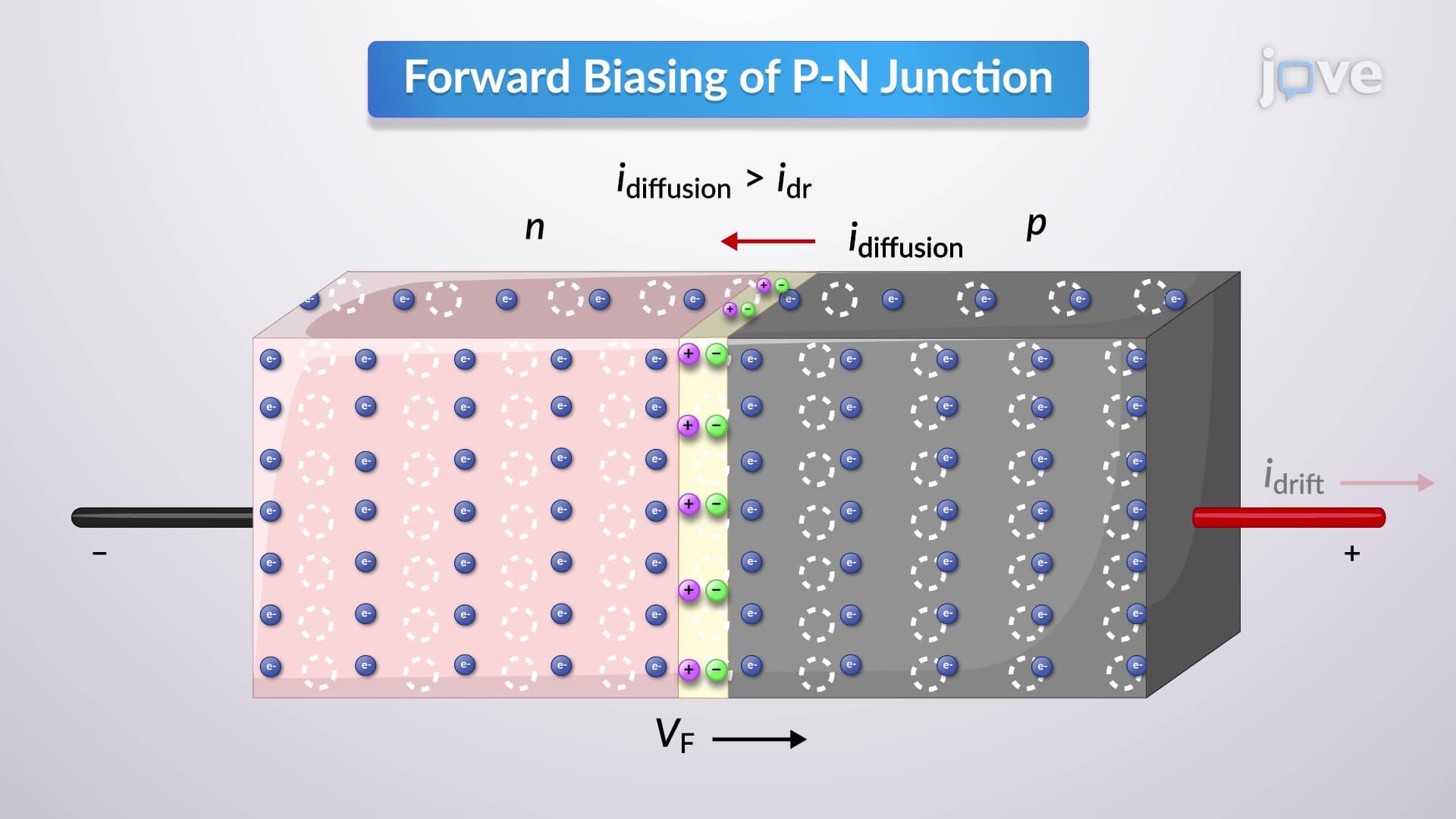
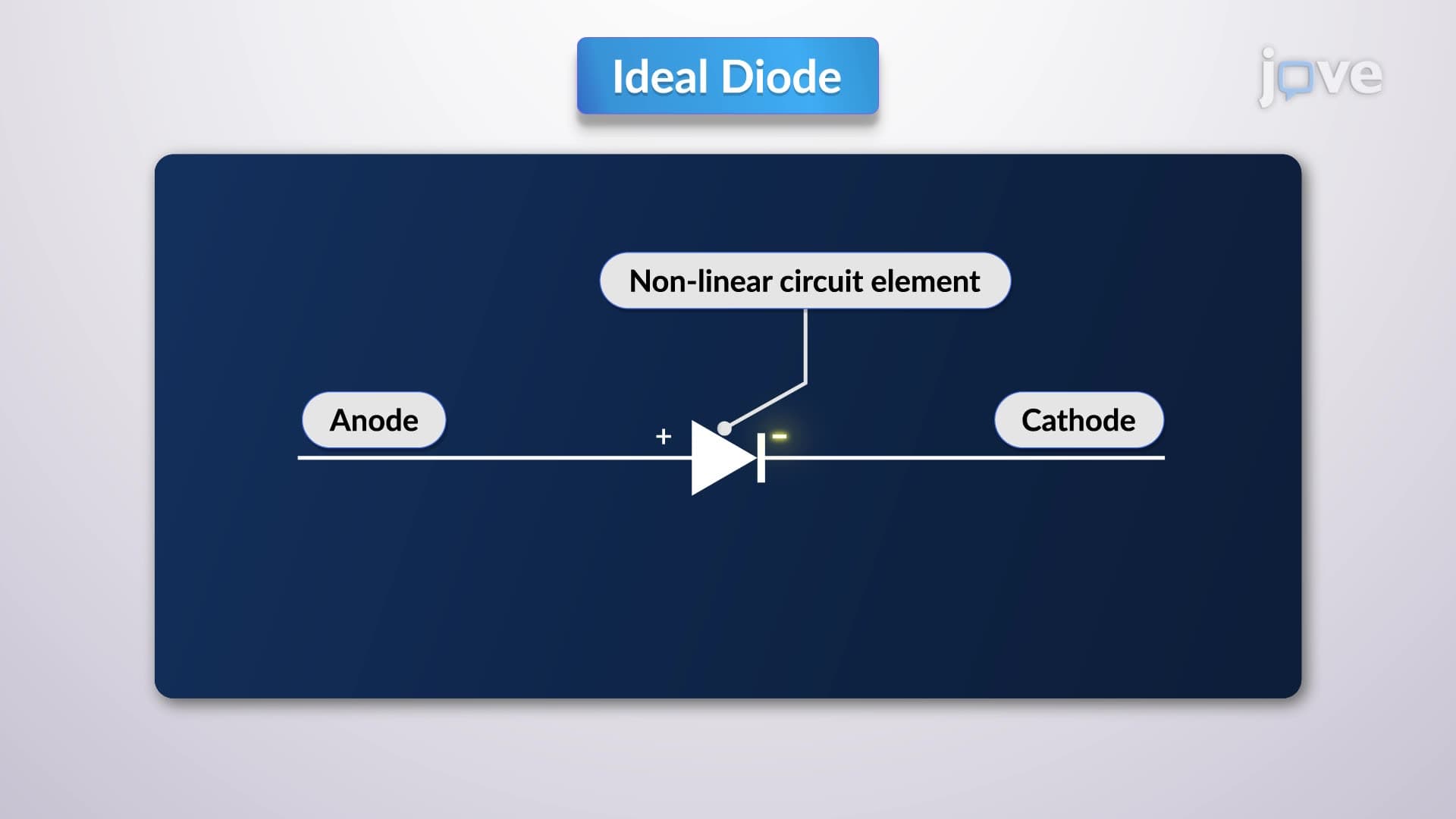
Forward biasing applies positive voltage to the metal while grounding the semiconductor, effectively lowering the metal's Fermi level relative to the semiconductor. This reduction in barrier height allows electrons to flow more easily from semiconductor to metal, creating substantial current flow. Texas Instruments' voltage regulators rely on this principle to maintain stable power supply in electronic circuits.
Reverse biasing raises the metal's Fermi level, increasing the barrier height and blocking most electron flow. However, some high-energy electrons still overcome this barrier, producing small reverse current-critical for understanding photodiode operation in medical imaging equipment used in US hospitals.
Understanding Fermi level basics helps explain why Silicon Valley companies like Intel design transistors with specific metal-semiconductor contacts. Ohmic contacts, with minimal barriers, enable low-resistance connections essential for computer processors. Meanwhile, Schottky barriers create the rectifying behavior needed in power supply circuits.
This Fermi level study guide material appears frequently on college semiconductor physics exams and graduate school qualifying tests. Students preparing for electrical engineering coursework at institutions like MIT or Stanford must master these concepts to succeed in advanced device physics courses.
Related Micro-courses