Loading video…


 11 Concepts
 9.9K views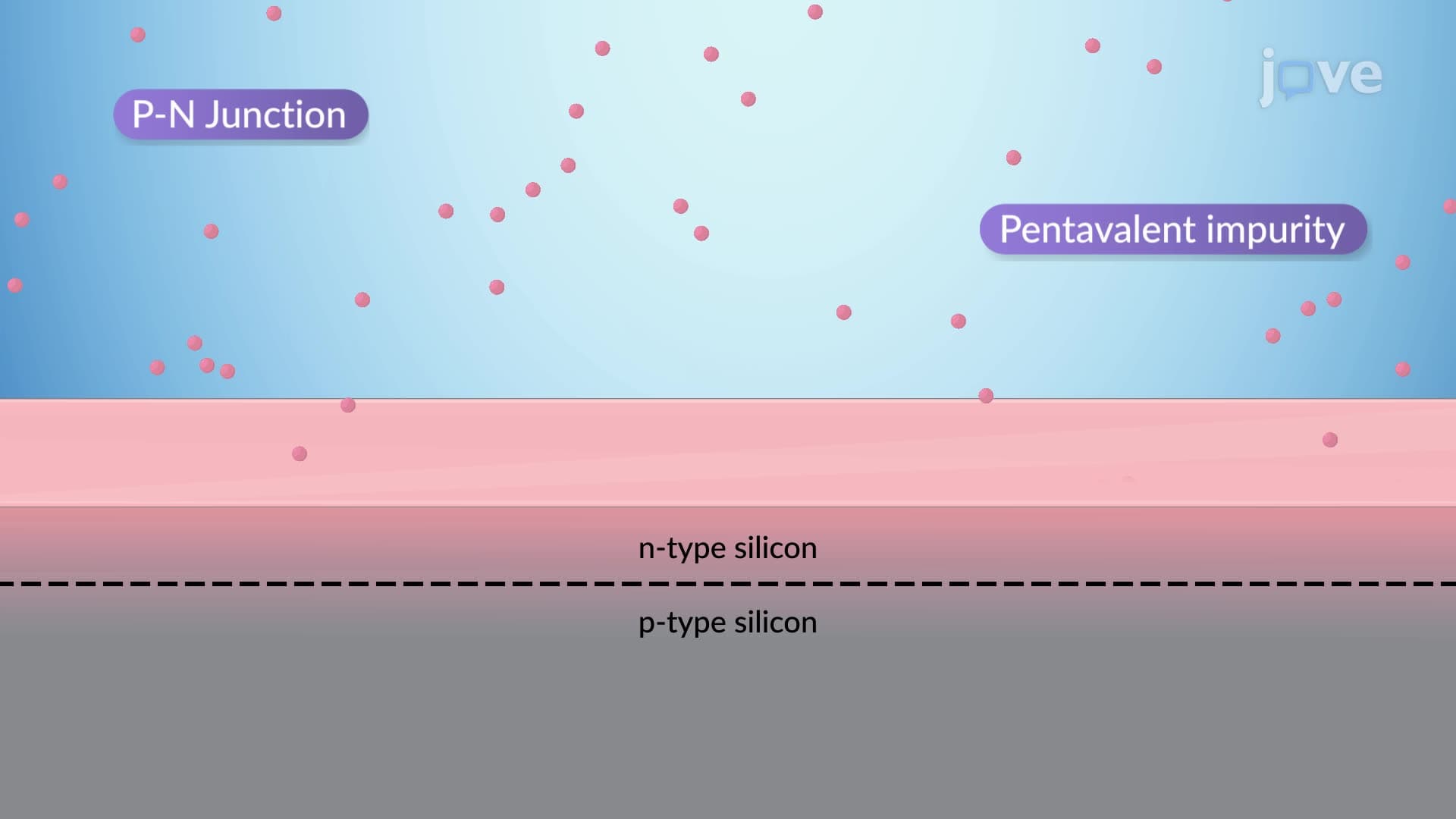

Video Summary: What Is P N Junction
Ever wondered how solar panels on US highways power streetlights without being plugged into the electrical grid? The secret lies in understanding the biasing of p n junction, a fundamental semiconductor concept that converts light directly into electricity. A p n junction forms when p-type and n-type silicon materials meet, creating a depletion region with an electric field that controls current flow. This same principle powers everything from LED traffic signals in New York City to solar arrays across California. Watch the full video on JoVE Coach to master this concept with expert-led visuals and step-by-step explanations.
A p n junction represents one of the most fundamental building blocks in modern electronics, forming the basis for diodes, solar cells, and transistors found in everything from smartphones to electric vehicle charging stations across the United States. The junction forms when p-type silicon (doped with trivalent atoms like boron) directly contacts n-type silicon (doped with pentavalent atoms like phosphorus). This seemingly simple interface creates a complex region with unique electrical properties that enable controlled current flow.
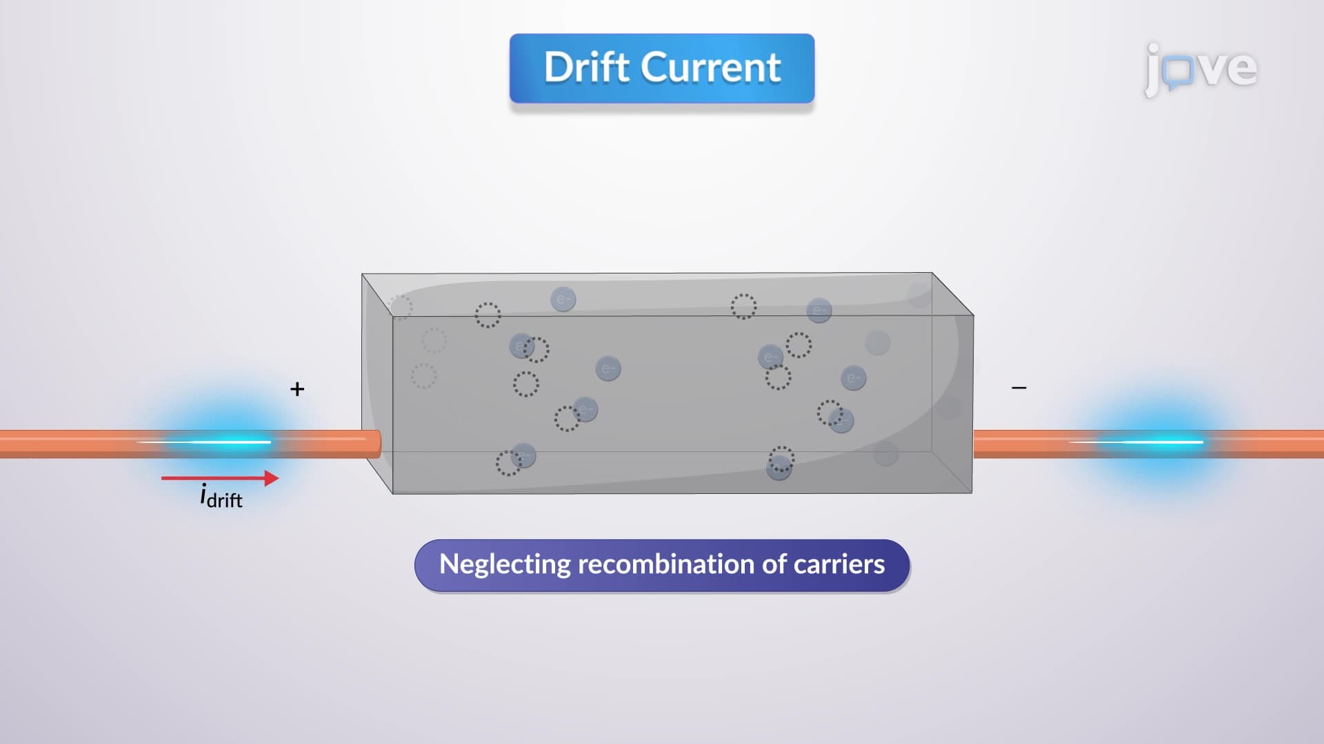
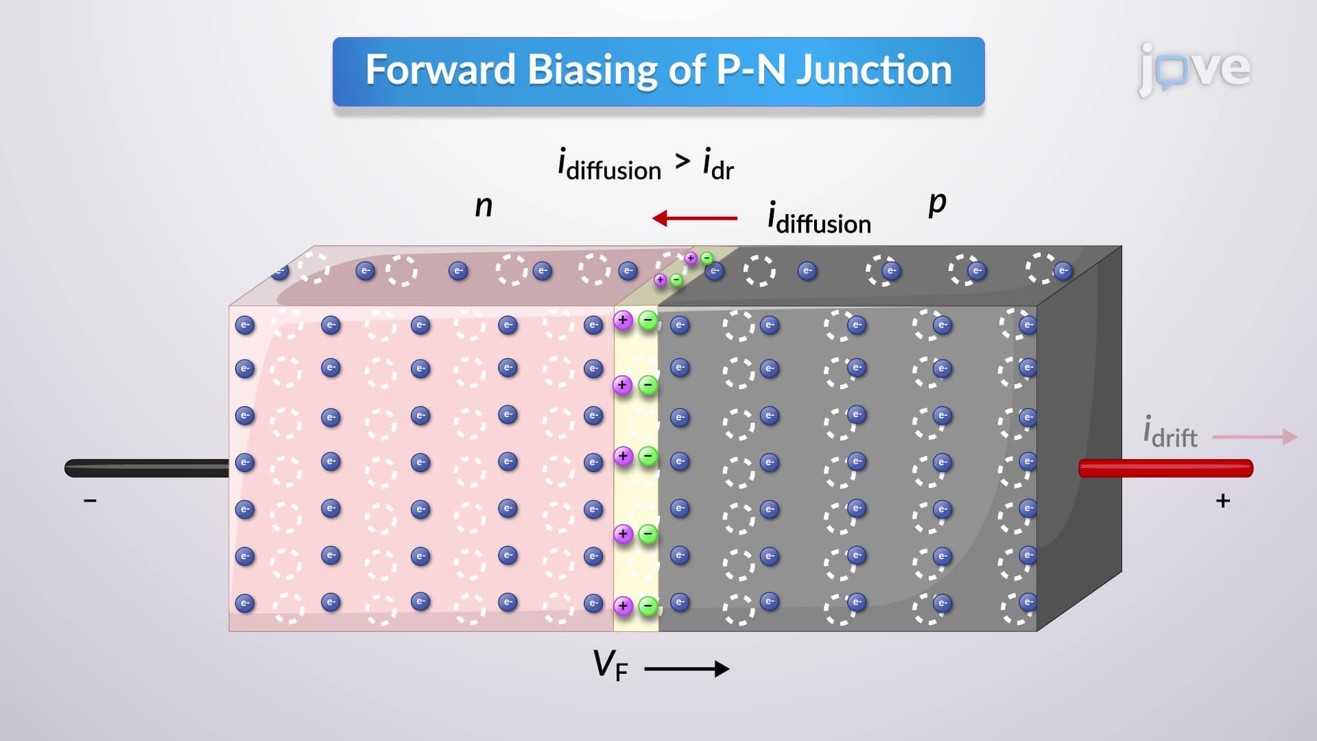
When p-type and n-type materials first contact, a concentration gradient drives charge carriers across the boundary. Holes from the p-side diffuse toward the n-side, while electrons move from n-type to p-type material. This initial diffusion creates the diffusion current, but simultaneously leaves behind immobile ionized atoms-positive ions on the n-side and negative ions on the p-side. These fixed charges establish an internal electric field pointing from n-type to p-type material.
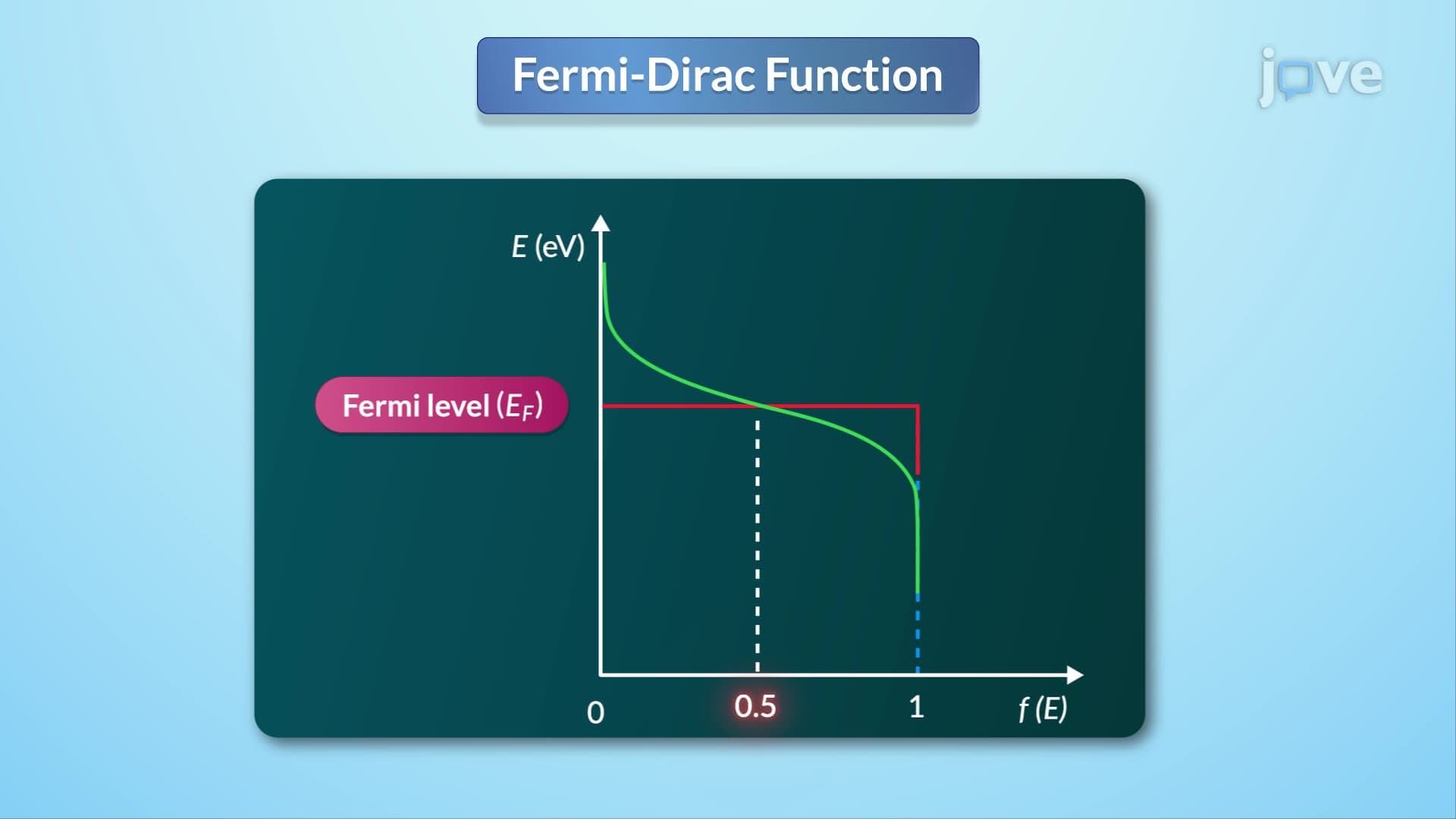
Understanding biasing of p n junction behavior becomes crucial for AP Physics students and college engineering majors. The electric field strength increases until it creates sufficient drift current to exactly balance the diffusion current. At this equilibrium, the net current across the junction equals zero, and the Fermi energy level becomes constant throughout the structure.
The region where mobile charge carriers have been depleted forms the aptly named depletion region or space charge region. This zone typically extends 0.1 to 1 micrometer on each side of the junction, depending on doping concentrations. Within this region, the electric field reaches strengths of 10^4 to 10^5 volts per centimeter-comparable to the breakdown fields in air.
For students preparing for the MCAT or college physics exams, recognizing that the depletion region acts like a variable capacitor becomes essential. When external voltage is applied (forward or reverse bias), the depletion width changes, altering the junction's electrical characteristics. This principle enables solar panels at installations like the Ivanpah Solar Power Facility in California to convert sunlight into electricity with over 20% efficiency.
Modern semiconductor devices rely heavily on controlled p n junction behavior. LED street lighting systems throughout US cities use forward-biased p n junctions to emit light when electrons recombine with holes. Conversely, photodiodes in fiber optic communication networks spanning from coast to coast operate under reverse bias to detect optical signals with minimal noise.
Students studying for AP Physics C or introductory electrical engineering courses should understand that biasing of p n junction concepts extend far beyond theoretical knowledge. These principles directly apply to photovoltaic systems, electronic circuit analysis, and semiconductor device physics that appear regularly on standardized exams and professional certification tests.
Related Micro-courses