Loading video…


 11 Concepts
 9.9K views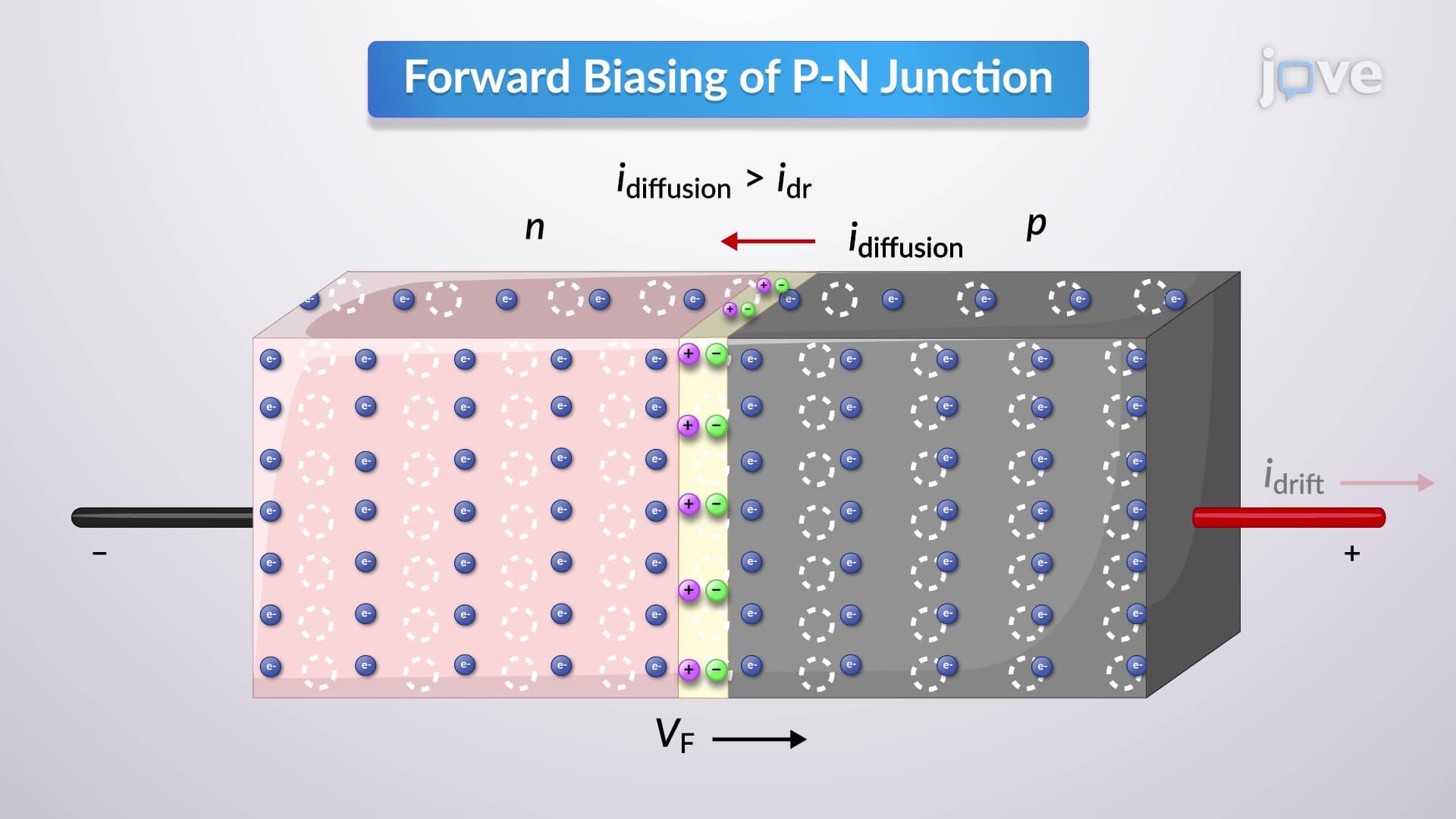

Video Summary: Biasing of P N Junction Explained
Ever wonder why your smartphone's LED indicator only glows when current flows in one direction? Metal semiconductor junctions form the foundation of countless electronic devices, from the LED notifications on iPhones to traffic lights across American highways. The biasing of P N junction explained reveals how applying voltage in forward or reverse direction controls current flow and light emission. Understanding this principle is crucial for grasping how modern electronics function in everything from Tesla's electric vehicles to NASA's space equipment. Watch the full video on JoVE Coach to master this concept with expert-led visuals and step-by-step explanations.
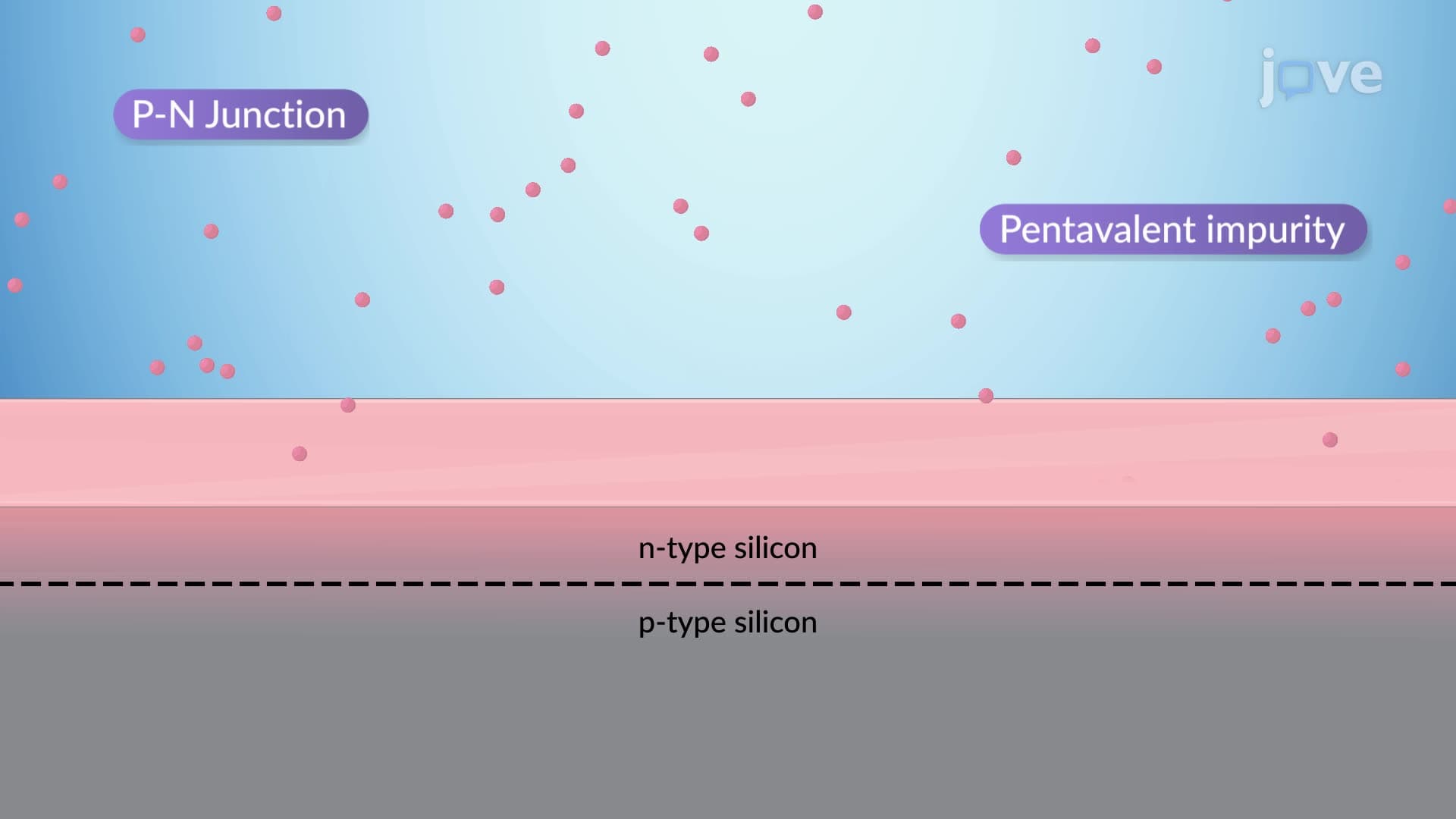
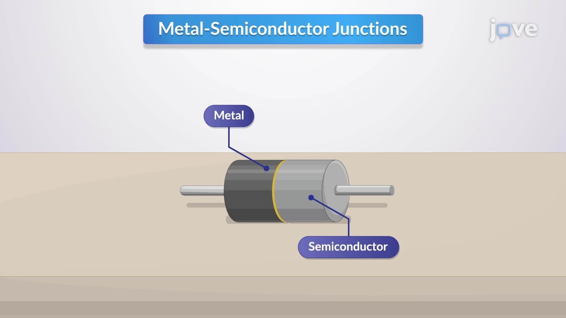
Metal semiconductor junctions represent one of the most fundamental concepts in solid-state electronics, forming the backbone of devices from simple diodes to complex integrated circuits. When we examine types of metal semiconductor junctions, P-N junctions stand out as the most widely studied and applied configuration. These junctions occur at the interface between P-type (hole-rich) and N-type (electron-rich) semiconductor materials, creating a depletion region that controls current flow.
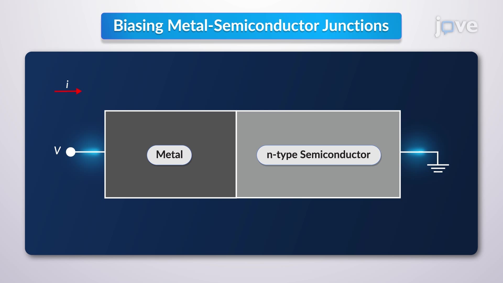
In forward biasing, engineers connect the positive terminal of a voltage source to the P-side and the negative terminal to the N-side of the junction. This configuration is essential in applications ranging from LED displays in Times Square billboards to the indicator lights in medical equipment at Johns Hopkins Hospital. The applied voltage opposes the built-in junction potential, effectively reducing the barrier width that normally prevents current flow.
This reduction in barrier width dramatically increases majority carrier diffusion. Electrons from the N-side diffuse toward the P-side, while holes from the P-side move toward the N-side. When these charge carriers recombine in the junction region, they release energy in the form of photons-the fundamental mechanism behind LED operation. This principle appears frequently on AP Physics exams and college-level electrical engineering courses, particularly when students analyze semiconductor device characteristics.
Reverse biasing creates the opposite effect by connecting the positive terminal to the N-side and negative terminal to the P-side. This configuration increases the junction potential, widening the depletion region and severely restricting majority carrier flow. The result is a minimal current consisting primarily of minority carriers-a concept crucial for understanding photodiode operation in solar panels manufactured by companies like First Solar in Ohio.
When reverse bias voltage exceeds a critical threshold, junction breakdown occurs, causing a sudden increase in current flow. This phenomenon, while potentially destructive in some applications, is deliberately utilized in Zener diodes for voltage regulation in power supplies. Understanding these breakdown mechanisms is essential for MCAT preparation, particularly in questions related to medical device electronics, and frequently appears in electrical engineering coursework at institutions like MIT and Stanford.
The metal semiconductor junctions overview encompasses these biasing principles as fundamental building blocks for more complex devices, making this knowledge indispensable for students pursuing STEM careers in the rapidly evolving electronics industry.
Related Micro-courses