13 Concepts
11 Concepts
9 Concepts
8 Concepts
13 Concepts
16 Concepts
9 Concepts
11 Concepts
15 Concepts
11 Concepts
14 Concepts
20 Concepts
11 Concepts
7 Concepts
5 Concepts
7 Concepts
10 Concepts
7 Concepts
7 Concepts
5 Concepts
9 Concepts
7 Concepts
7 Concepts
7 Concepts
10 Concepts
4 Concepts
7 Concepts
6 Concepts
8 Concepts
9 Concepts
7 Concepts
5 Concepts
5 Concepts
Semiconductor basics form the foundation of modern electronics, covering energy band theory, carrier behavior, and junction physics. This comprehensive course explores semiconductor physics fundamentals from atomic structure to device applications, including p-n junctions powering American solar farms and LED streetlights. Master the basic properties of semiconductor materials essential for understanding transistors, diodes, and integrated circuits used in smartphones, computers, and renewable energy systems. JoVE Coach guides students through complex concepts with clear visualizations.
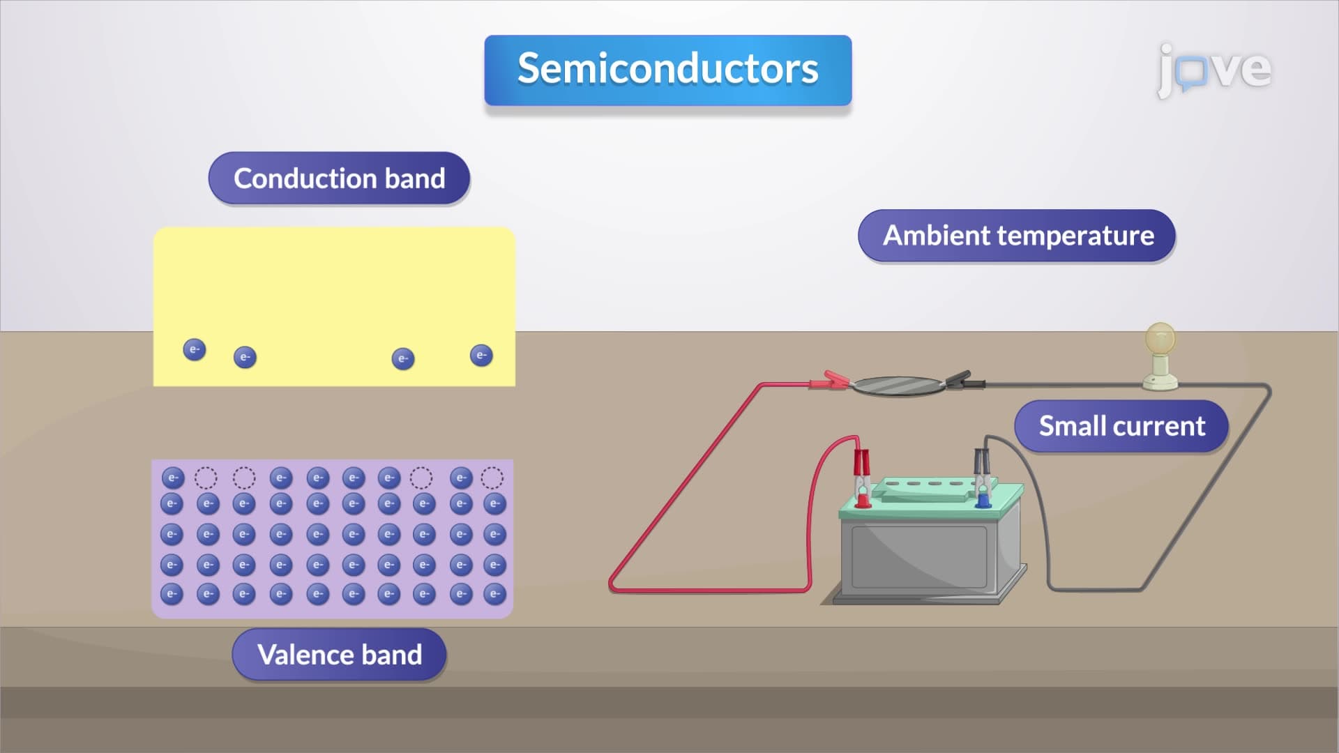
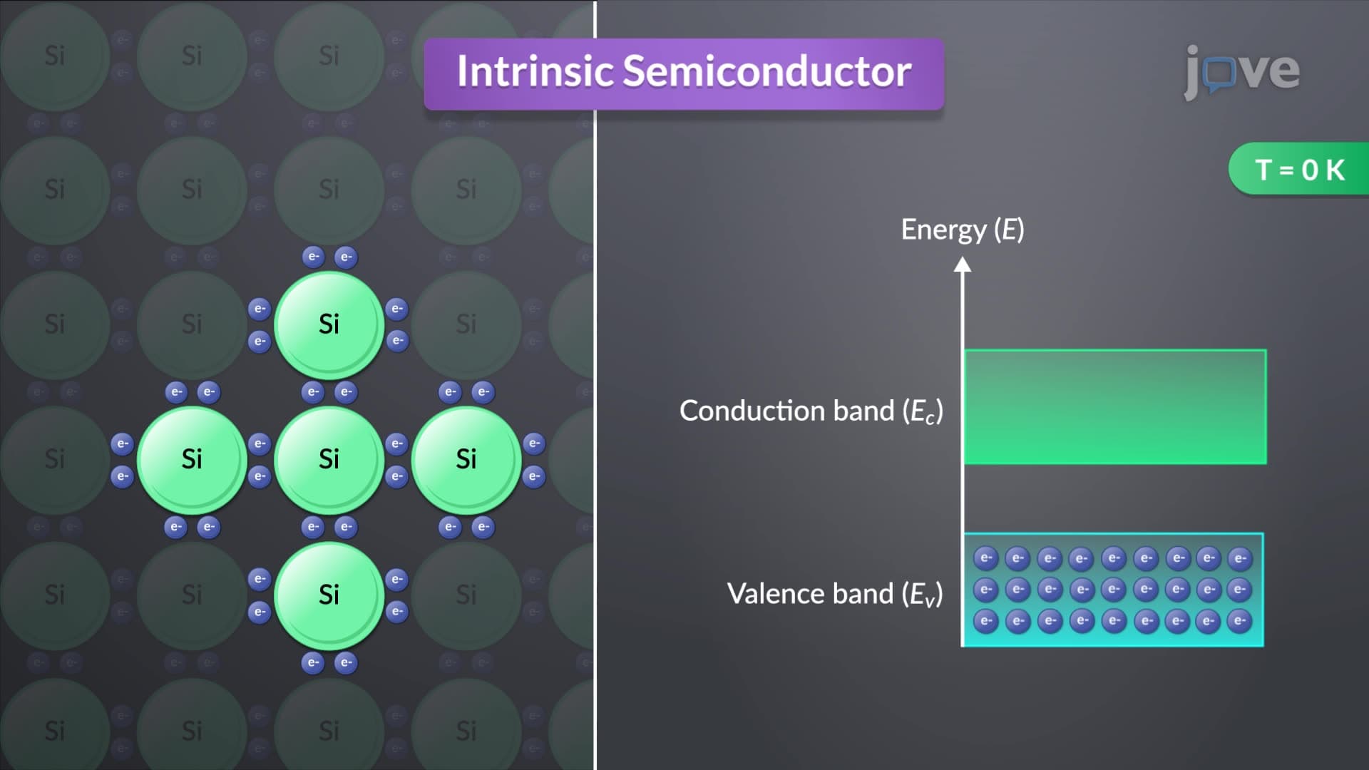
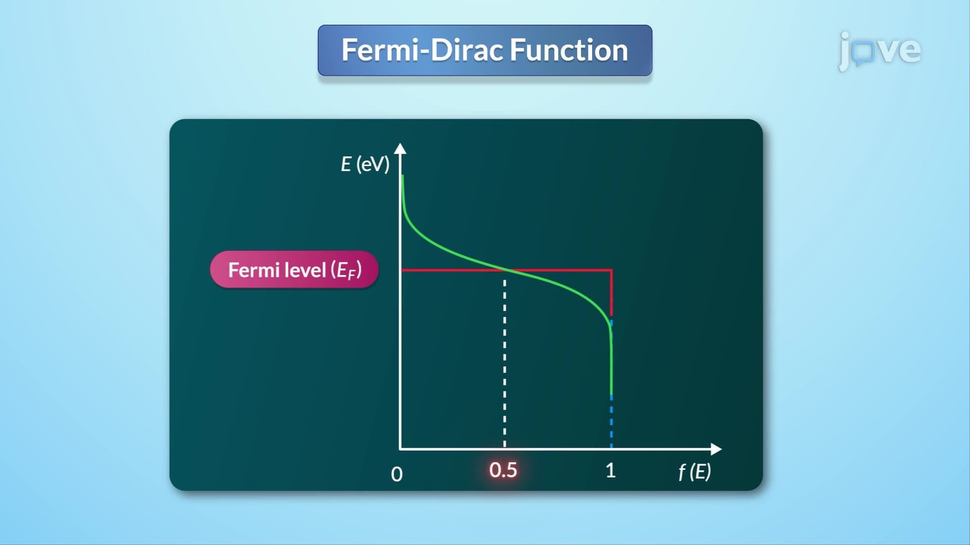
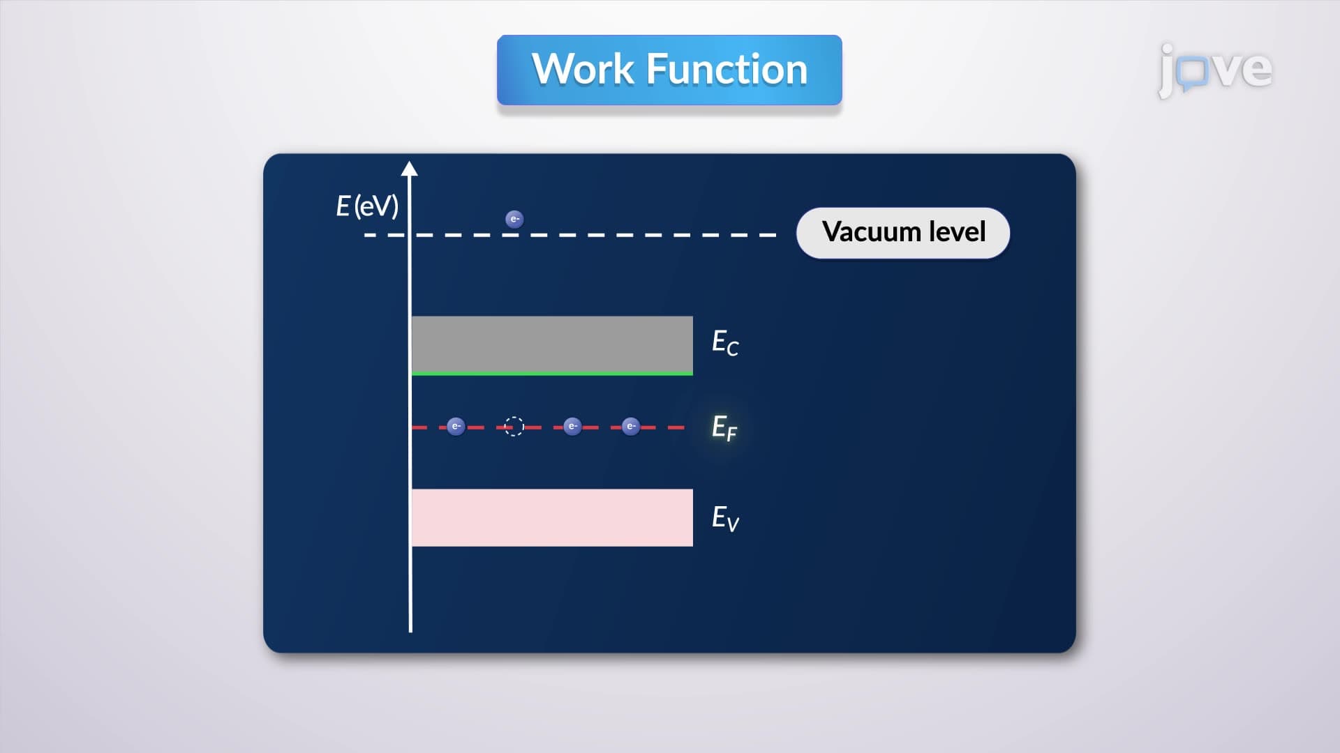
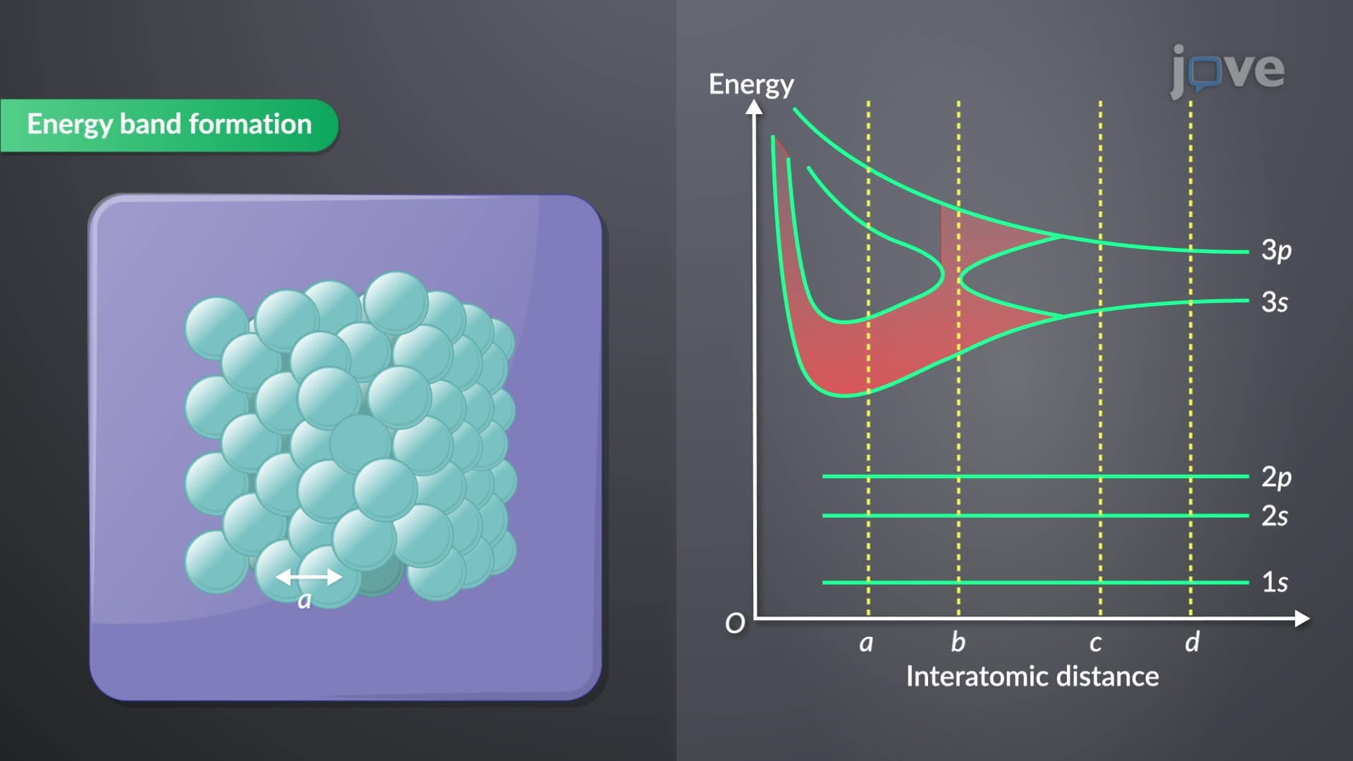
1. Energy Band Theory in Solids When atoms combine to form crystalline materials like silicon wafers used in computer processors, their individual energy levels merge into continuous energy bands. The valence band contains electrons bound to atoms, while the conduction band allows free electron movement. The energy gap between these bands determines material properties-metals have overlapping bands enabling conductivity, insulators like glass have large gaps preventing current flow, and semiconductors like silicon have moderate gaps around 1.1 eV, allowing controlled conductivity for electronic devices.
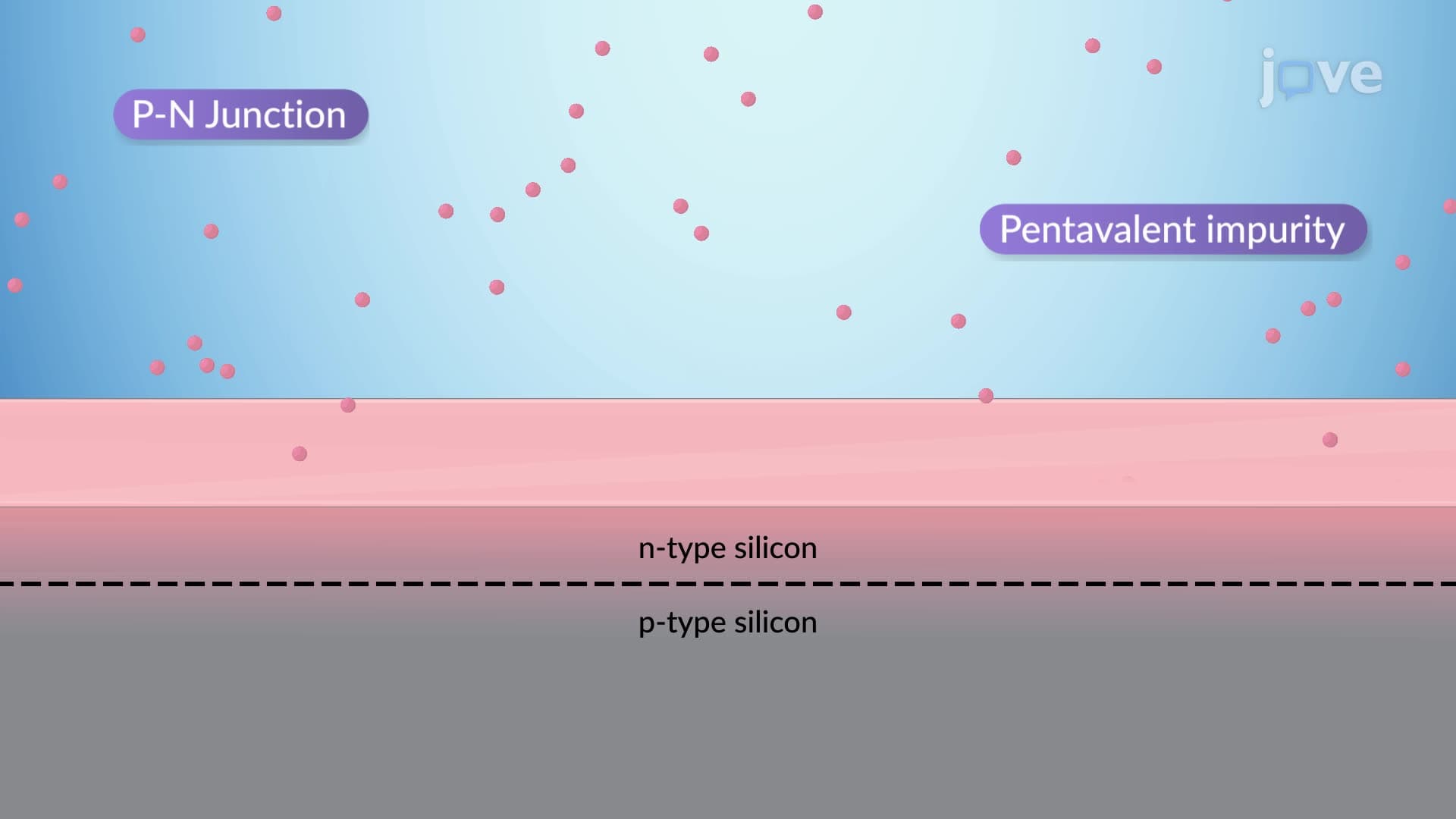
2. Intrinsic vs. Extrinsic Semiconductors Pure silicon represents an intrinsic semiconductor with equal electron and hole concentrations at room temperature. However, American semiconductor manufacturers like Intel deliberately introduce impurities through doping to create extrinsic semiconductors. Adding phosphorus (pentavalent) creates n-type material with excess electrons, while boron (trivalent) produces p-type material with electron deficiencies called holes. This controlled doping enables precise electrical property modification essential for microprocessor fabrication.
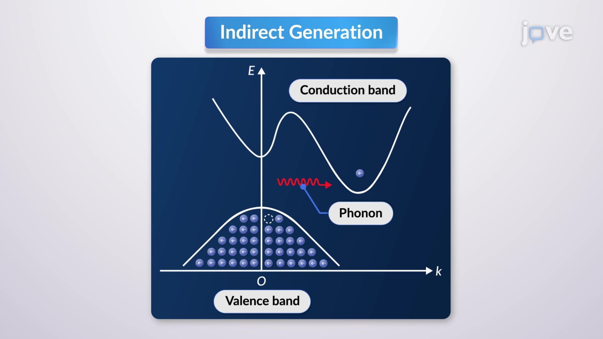
3. Carrier Generation and Recombination Semiconductor devices function through electron-hole pair creation and destruction. Thermal energy at room temperature generates carriers in materials like gallium arsenide used in high-speed communications. Photons from sunlight create carriers in solar panels, converting light energy to electricity. Recombination occurs when electrons fall back to the valence band, either releasing photons in LEDs or generating heat in power transistors. Understanding these processes enables optimization of semiconductor device performance and efficiency.
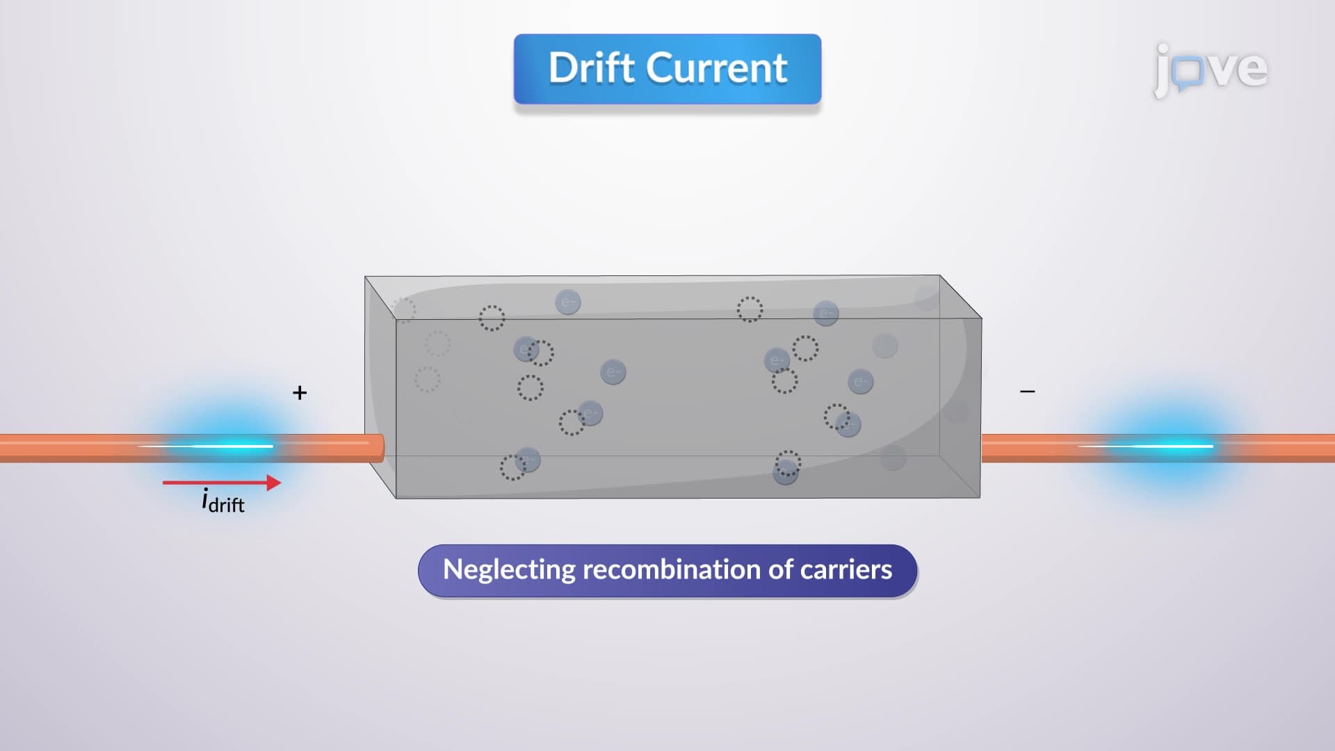
4. Carrier Transport Mechanisms Electric current flows through semiconductors via two primary mechanisms. Drift current results from applied electric fields accelerating charge carriers, similar to electrons flowing through copper wires. Diffusion current occurs when carriers move from high to low concentration regions, like sugar dissolving in water. Both mechanisms contribute to current flow in transistors and diodes. The mobility and diffusion coefficient relationships, described by Einstein's relation, determine how quickly carriers respond to electrical signals.
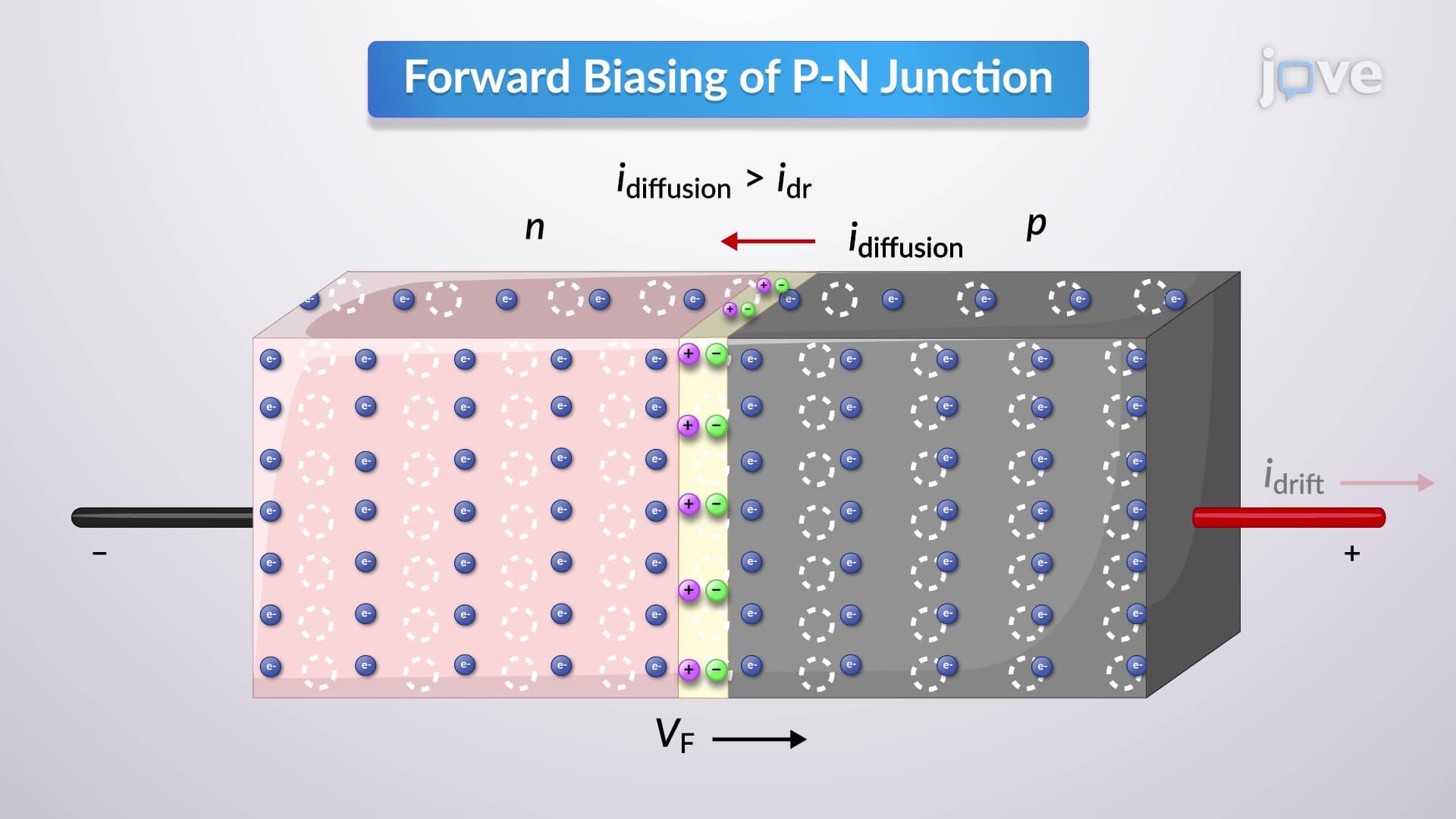
5. P-N Junction Physics and Applications Joining p-type and n-type materials creates the fundamental building block of modern electronics. At the junction boundary, electrons diffuse from n-type to p-type regions, creating a depletion zone with built-in electric field. This structure enables one-way current flow in diodes, light emission in LEDs used in traffic signals, and photovoltaic conversion in solar panels powering American homes. Forward biasing reduces the barrier for current flow, while reverse biasing blocks current except for small leakage components.
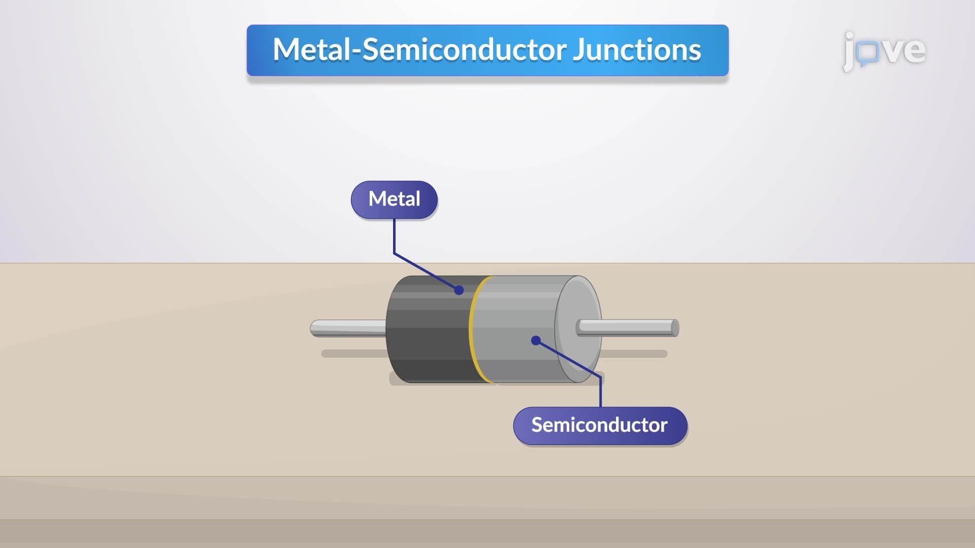
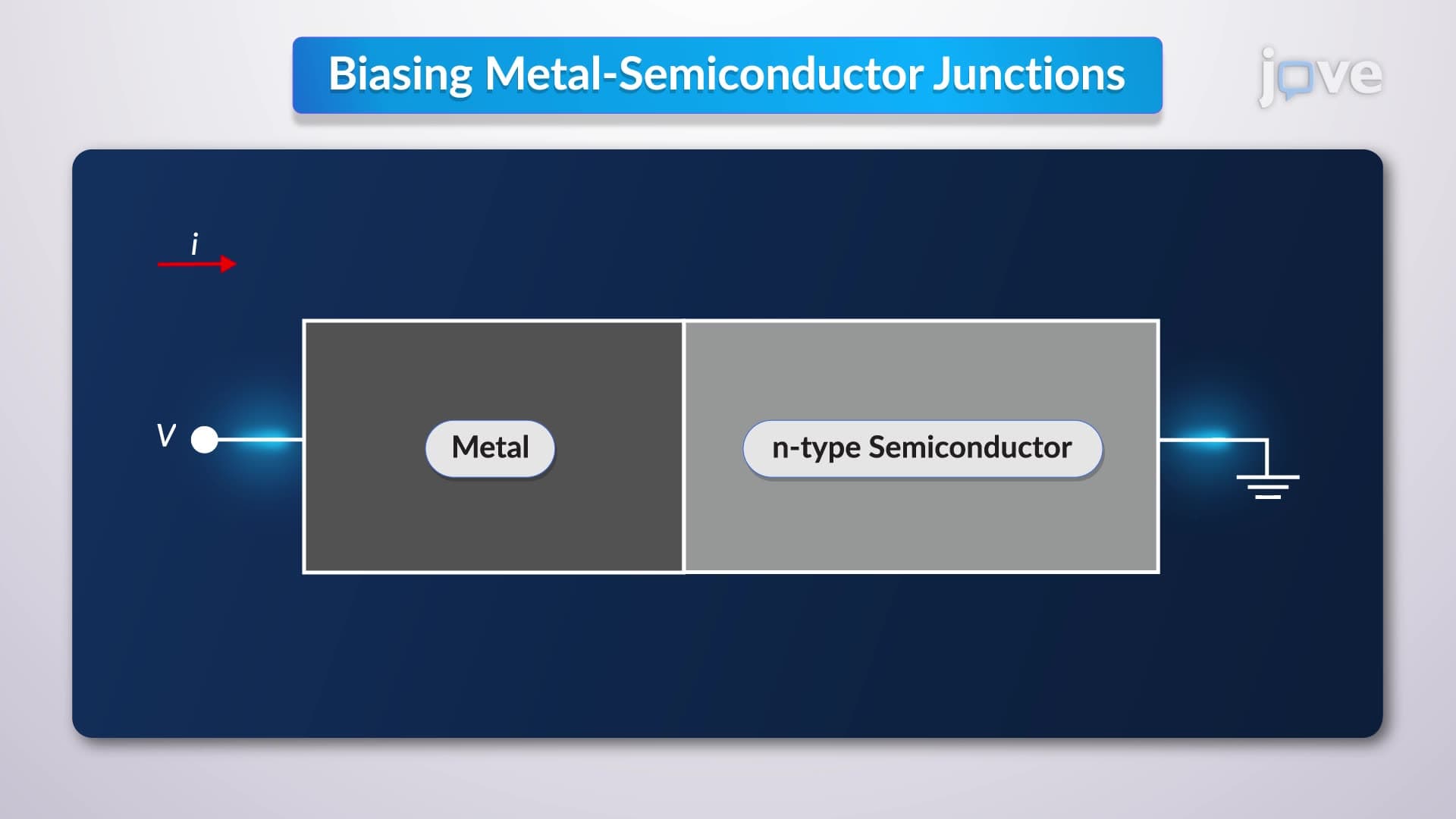
6. Metal-Semiconductor Contacts Contact between metals and semiconductors creates either Schottky or Ohmic junctions depending on their relative work functions. Schottky contacts form rectifying barriers useful in high-frequency diodes and solar cells, while Ohmic contacts provide low-resistance connections essential for transistor terminals. These junctions determine how effectively external circuits can inject or extract carriers from semiconductor devices. American manufacturers like Texas Instruments optimize these contacts for reliable integrated circuit operation across temperature variations.