Loading video…


 20 Concepts
 16.9K views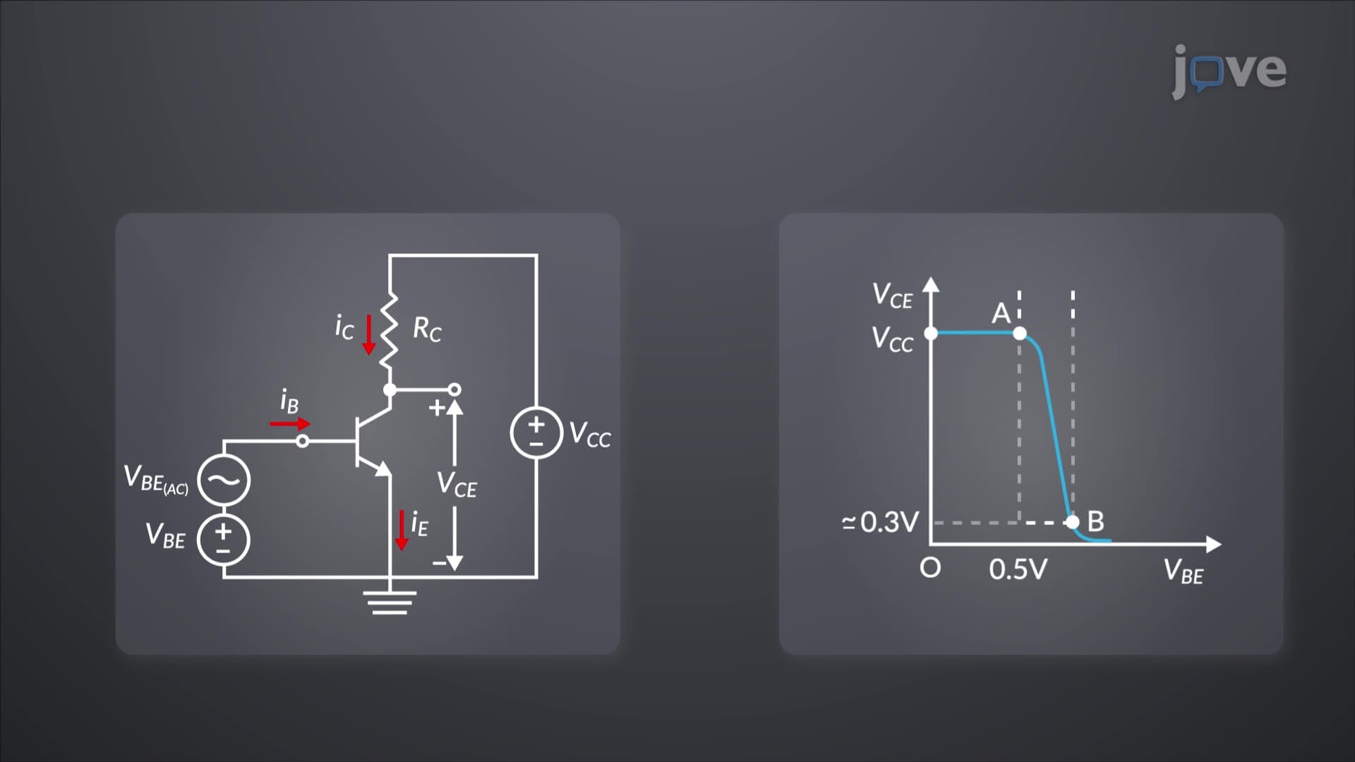

Video Summary: Small Signal Analysis of Bjt Amplifiers Explained
Did you know that the tiny amplifiers in your smartphone's audio circuit use the same small signal analysis principles found in NASA's Mars rover electronics? Field effect transistor circuits and BJT amplifiers both rely on small signal approximations to achieve precise linear amplification in everything from Texas Instruments' operational amplifiers to Qualcomm's 5G processors. Small Signal Analysis of BJT Amplifiers Explained demonstrates how engineers linearize exponential transistor behavior using thermal voltage approximations. Watch the full video on JoVE Coach to master this concept with expert-led visuals and step-by-step explanations.
Small signal analysis represents one of the most powerful techniques in analog electronics, enabling engineers to predict amplifier behavior with remarkable accuracy. This approach transforms the complex exponential relationship of bipolar junction transistors into manageable linear models, making circuit analysis feasible for practical applications.
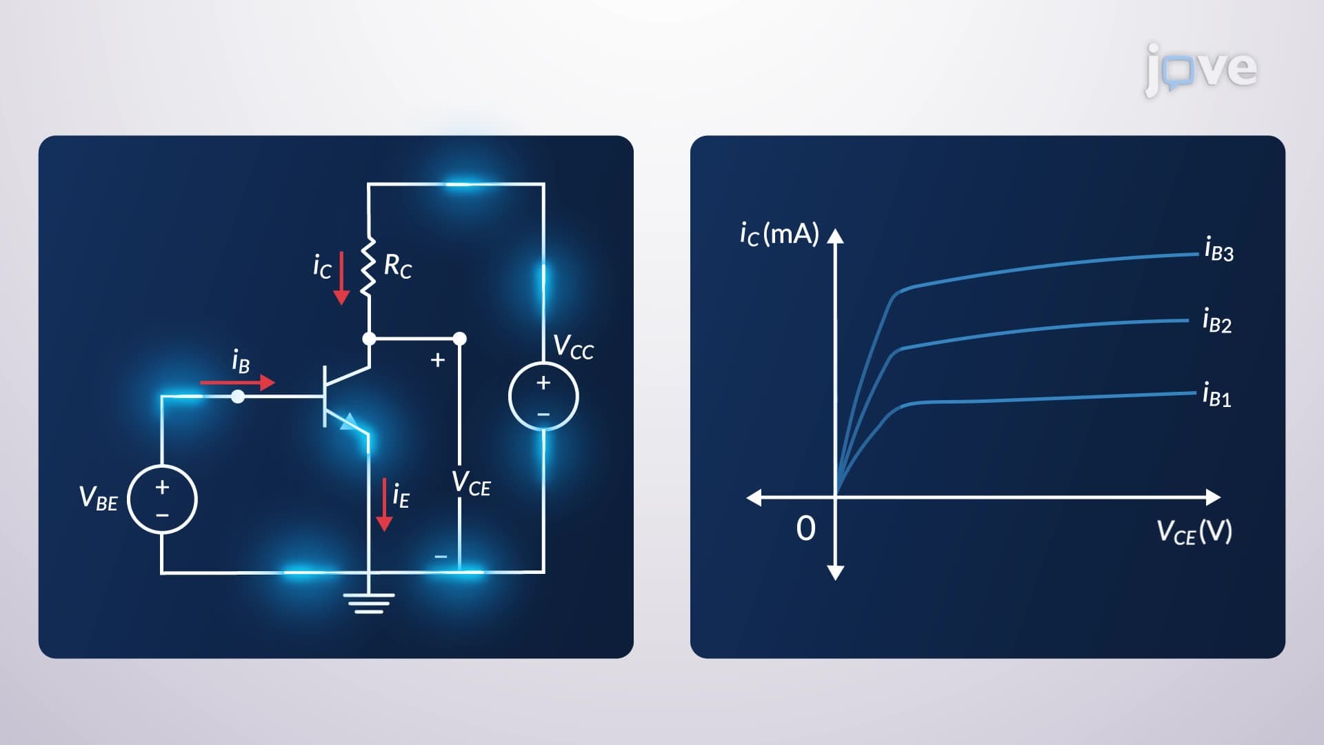
The fundamental concept revolves around the exponential relationship between base-emitter voltage and collector current: IC = IS × exp(VBE/VT). When signal variations remain small compared to thermal voltage (approximately 26 millivolts at room temperature), this exponential can be linearized using Taylor series expansion, creating the small signal approximation that drives modern amplifier design.
BJT transconductance (gm) represents the slope of the transfer characteristic at the operating point, mathematically expressed as gm = IC/VT. This parameter directly links DC bias conditions to AC performance, explaining why proper biasing is crucial in amplifier design. Unlike field effect transistor devices where transconductance depends on gate overdrive voltage, BJT transconductance scales linearly with collector current.
Major semiconductor companies like Analog Devices and Linear Technology leverage this predictable relationship in their precision amplifier designs. For instance, the classic LM741 operational amplifier uses carefully controlled bias currents to achieve consistent transconductance across temperature variations.
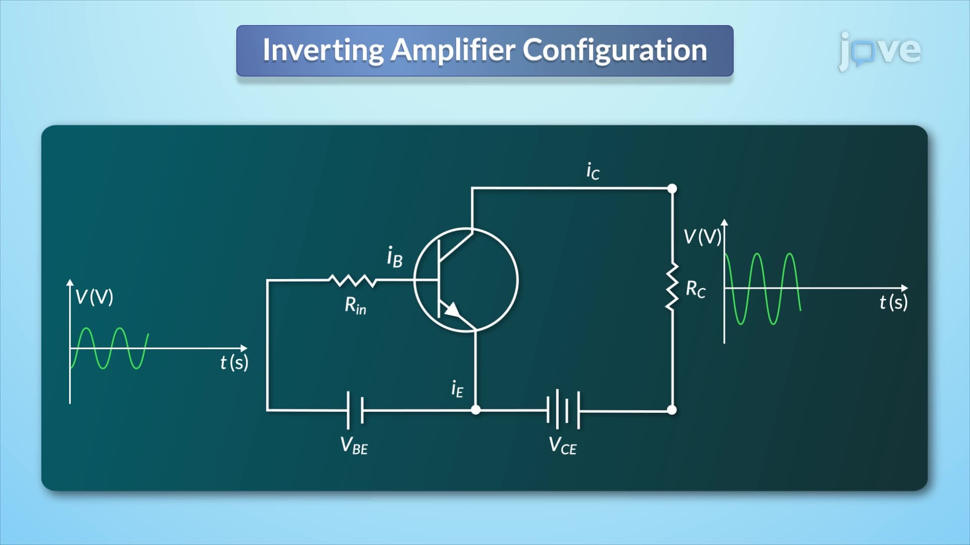
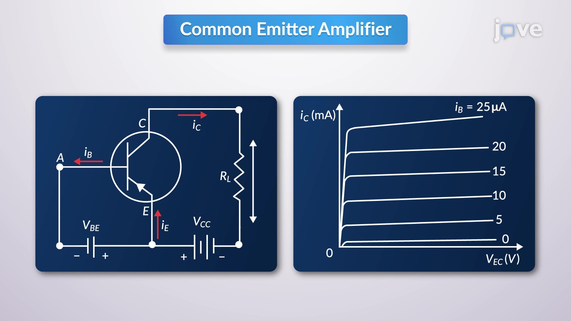
The negative voltage gain formula (Av = -gm × RL) reveals two critical amplifier characteristics. First, gain magnitude increases with both transconductance and load resistance, providing design flexibility. Second, the negative sign indicates 180-degree phase inversion-a signature characteristic of common-emitter configurations used extensively in audio amplifiers and signal processing circuits.
This phase relationship appears frequently on AP Physics exams and college electronics assessments, where students must predict output waveform polarity given input signals. Understanding this concept proves essential for analyzing feedback systems and oscillator circuits in advanced coursework.
The small signal base-emitter resistance (re = VT/IE) provides the final piece of the small signal model. This dynamic resistance, typically ranging from a few ohms to several hundred ohms depending on bias current, influences input impedance calculations and frequency response characteristics.
Modern RF amplifiers in cellular base stations and satellite communications rely heavily on these small signal parameters for impedance matching and noise figure optimization. Companies like Qorvo and Skyworks design their power amplifiers using these fundamental relationships to achieve the performance specifications required for 5G infrastructure.
Related Micro-courses