Loading subject page…


16,906 views

Video Summary: What Is Biasing of Fet
Ever wondered how your smartphone's processor switches billions of times per second? The secret lies in FET biasing-a fundamental technique that controls how Field Effect Transistors operate by applying specific voltages to their terminals. Just like the advanced chips powering Apple's latest iPhone processors, FET biasing determines whether these electronic switches turn "on" or "off" by manipulating the depletion regions within the semiconductor material. Watch the full video on JoVE Coach to master this concept with expert-led visuals and step-by-step explanations.
FET biasing represents the strategic application of DC voltages to Field Effect Transistor terminals to establish desired operating conditions. This fundamental concept determines how these semiconductor devices function as amplifiers, switches, or voltage-controlled resistors in countless electronic applications-from the microprocessors in Dell computers to the audio amplifiers in Marshall guitar amplifiers used across American music studios.
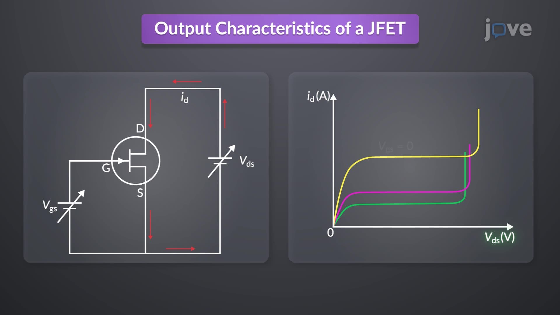
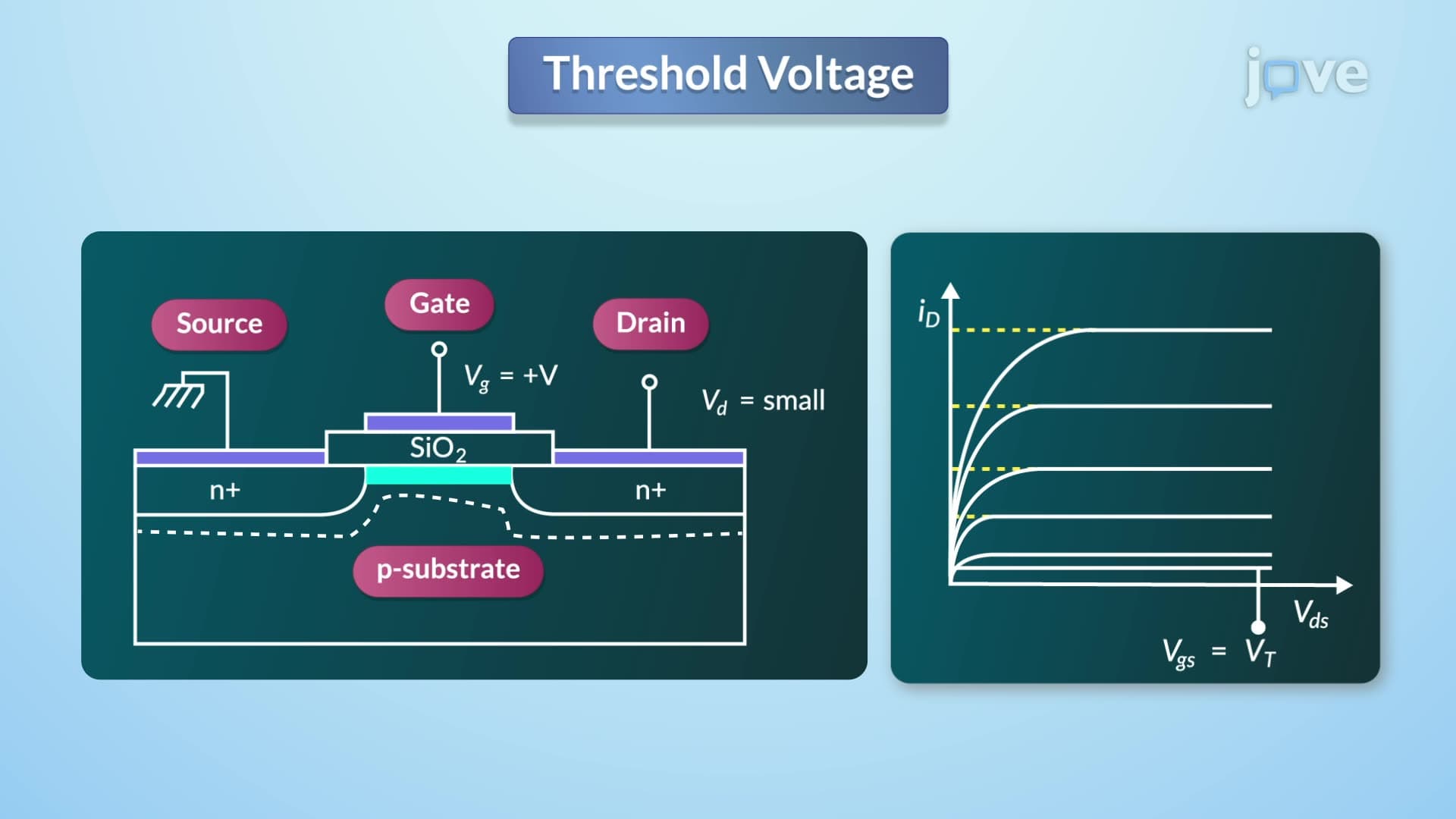
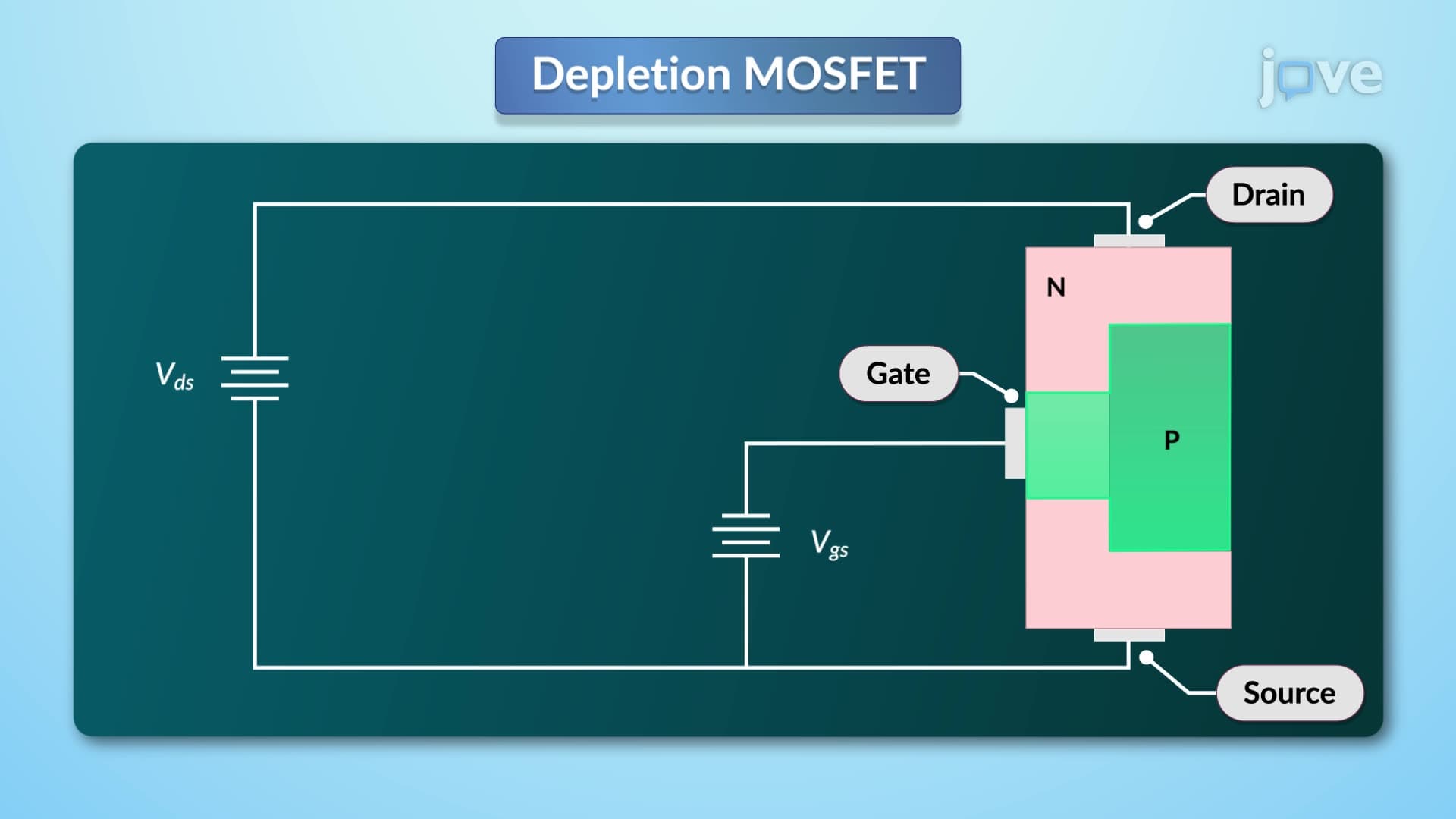
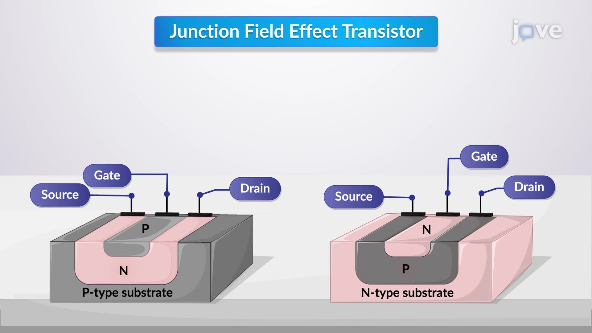
The biasing process in JFETs operates through voltage-controlled depletion region manipulation. In N-channel JFETs, applying a negative gate-to-source voltage creates an electric field that repels electrons from the channel region, effectively narrowing the conductive pathway. This reverse-bias condition expands the depletion region, increasing channel resistance and reducing current flow. Conversely, P-channel JFETs require positive gate voltages to repel holes and achieve similar current control through depletion region expansion.
The mathematical relationship governing this behavior involves the transconductance parameter, where small changes in gate voltage produce proportional changes in drain current. This voltage-current relationship makes FETs invaluable in precision applications like the analog-to-digital converters found in medical equipment manufactured by companies such as General Electric Healthcare.
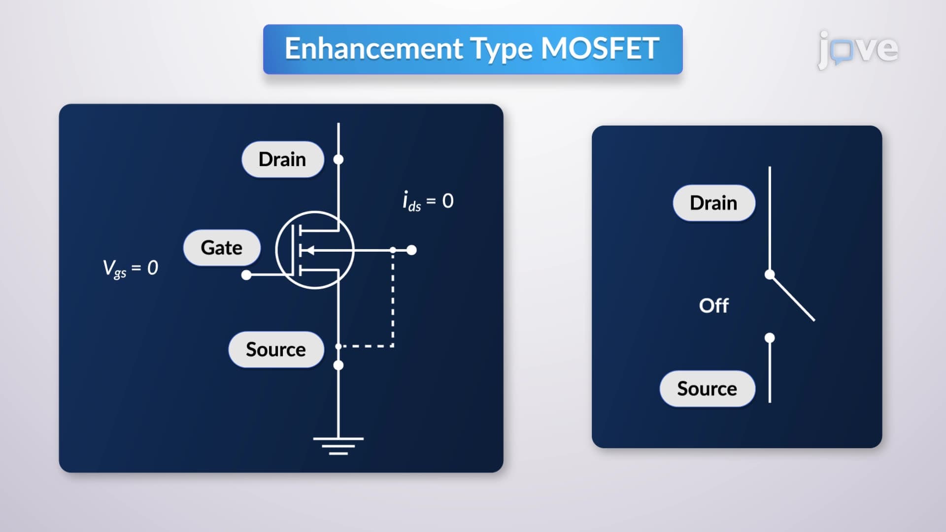
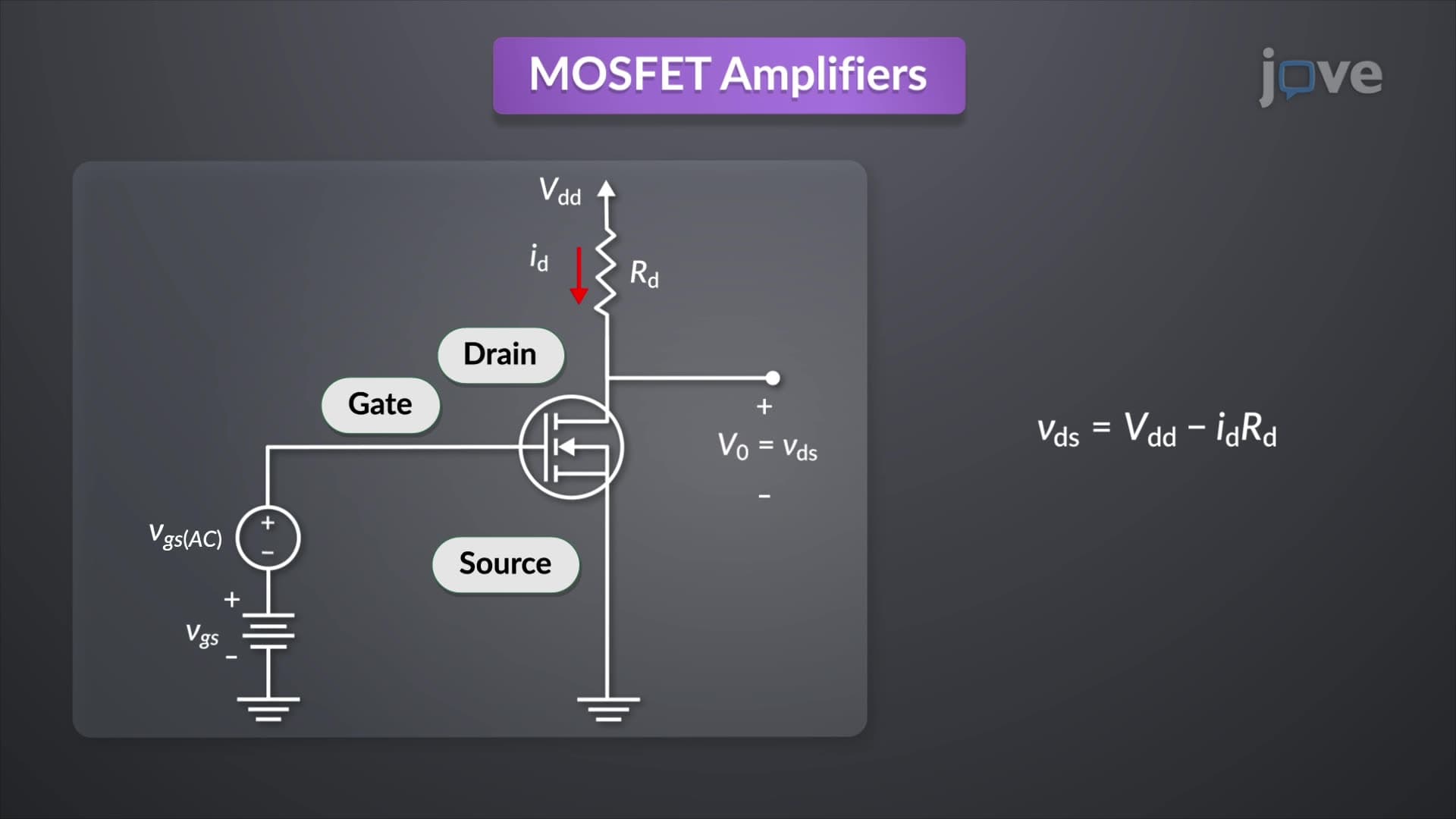
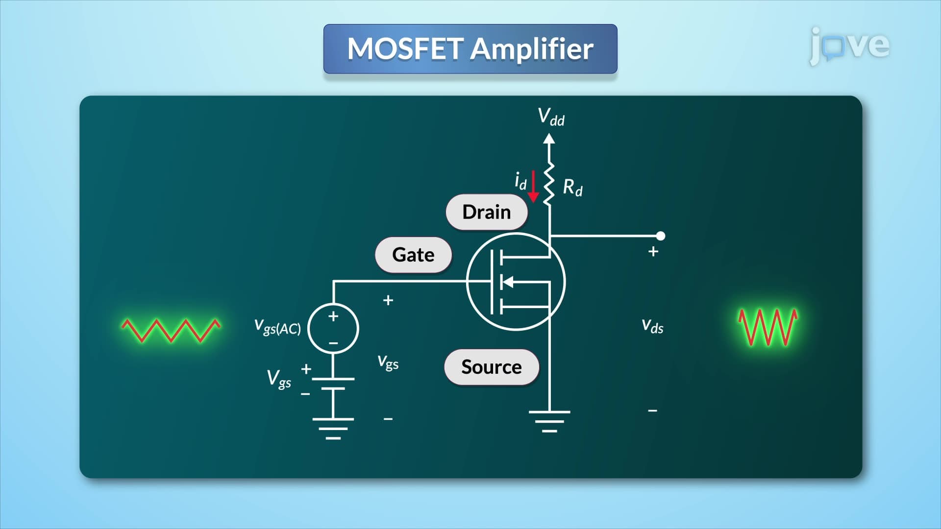
Proper FET biasing ensures transistors operate within their optimal regions for specific applications. In amplifier circuits commonly studied in university courses like those at MIT or Stanford, biasing establishes the quiescent operating point-the steady-state condition around which AC signals can swing without distortion. Engineers carefully select bias voltages to position the transistor in its linear region for amplification or at cutoff/saturation boundaries for digital switching.
Students preparing for Advanced Placement Physics exams often encounter FET biasing problems requiring analysis of voltage divider networks that provide stable bias conditions. These circuits typically incorporate feedback mechanisms to maintain consistent operating points despite temperature variations or component tolerances-critical considerations in aerospace applications developed by companies like Boeing or Lockheed Martin.
Contemporary FET biasing techniques enable the sophisticated power management systems found in everything from Tesla electric vehicles to data centers operated by Amazon Web Services. Advanced biasing schemes allow dynamic adjustment of transistor operating points, optimizing power consumption while maintaining performance-a principle essential for extending battery life in portable devices and reducing energy costs in large-scale computing infrastructures.
Related Micro-courses