Loading subject page…

- Electrical Engineering
- Basics of Semiconductors
- Carrier Transport
Micro-course: Basics of Semiconductors
9,886 views
Learn key concepts and earn your certificate.

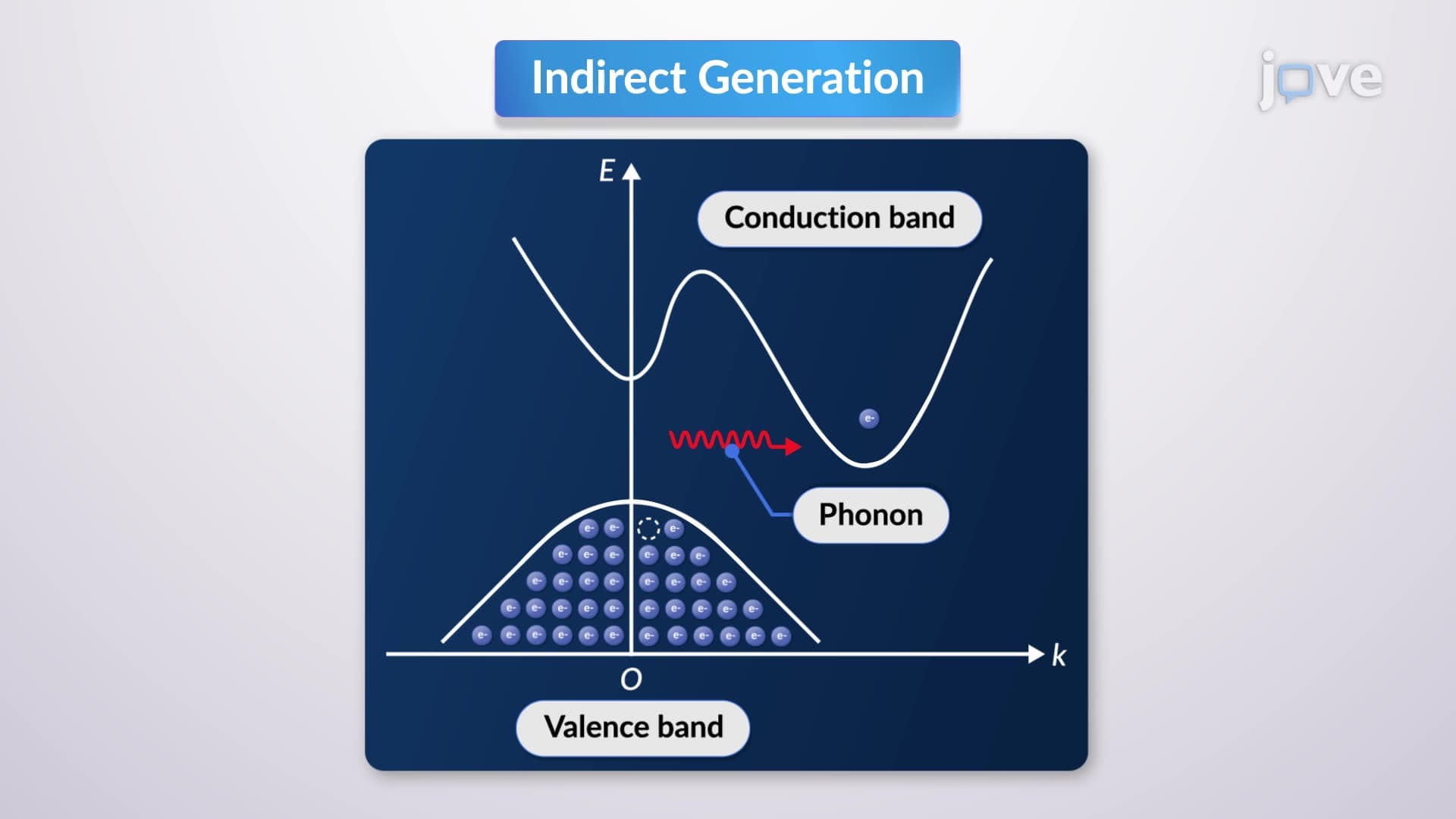
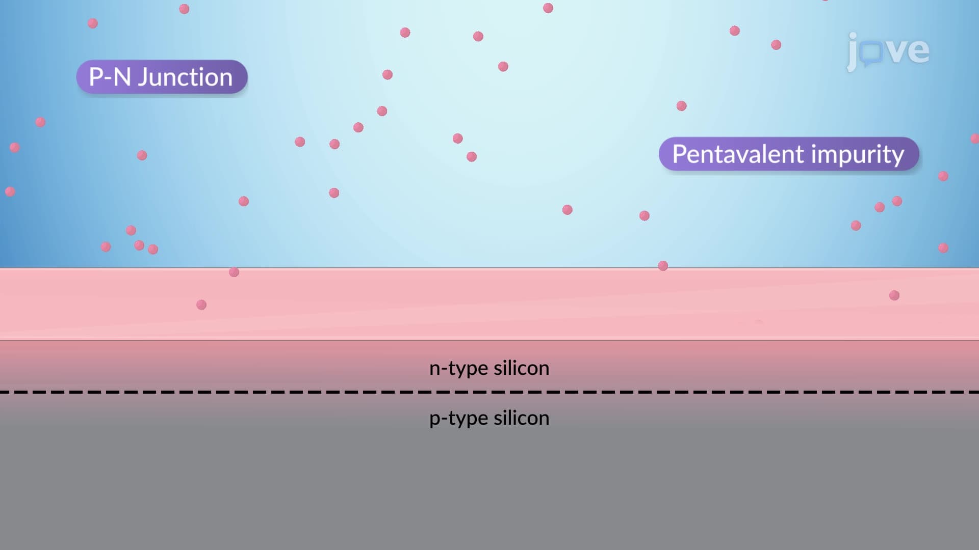
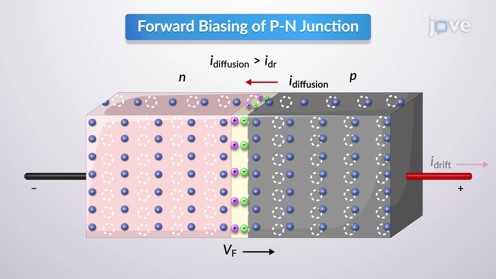
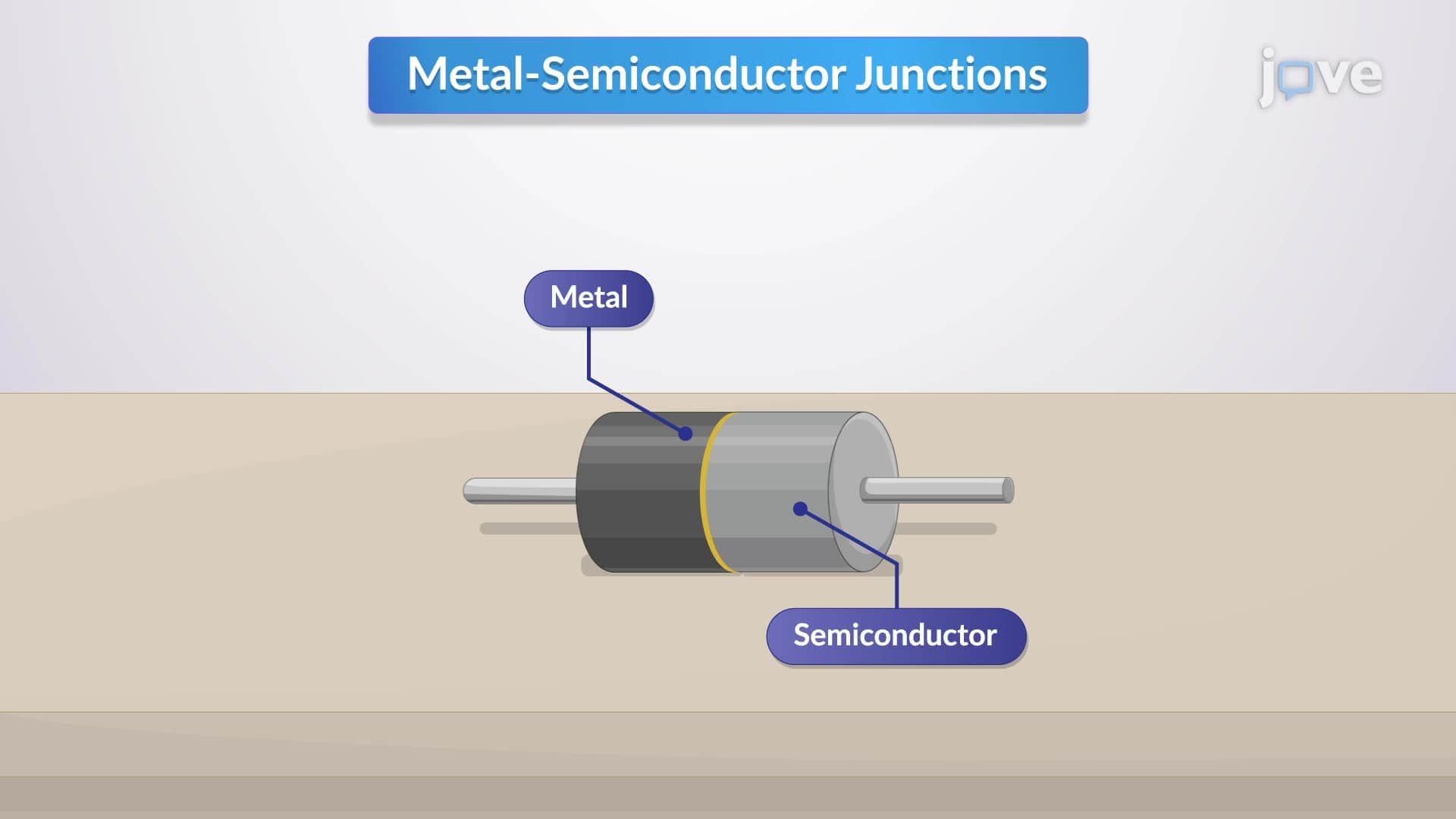
Carrier Transport

00:00
01:21
Video Summary: What Is Carrier Transport
Every smartphone, LED light, and solar panel in your home depends on the precise movement of electrons and holes through semiconductor materials. Understanding p n junction behavior starts with mastering what is carrier transport, the fundamental process that enables current flow in electronic devices. Silicon Valley's entire $500 billion semiconductor industry relies on engineers who can predict and control how charged particles drift under electric fields and diffuse across concentration gradients. Watch the full video on JoVE Coach to master this concept with expert-led visuals and step-by-step explanations.
- Understand what is carrier transport and how it creates current flow through drift and diffusion mechanisms in semiconductor devices
- Identify the relationship between electric fields, carrier mobility, and drift velocity in p n junction operation
- Analyze how concentration gradients drive diffusion current from high to low carrier density regions
- Compare drift current density equations for electrons versus holes using charge density and mobility parameters
- Evaluate the Einstein relation connecting diffusion coefficient to carrier mobility in semiconductor materials
- Apply combined drift and diffusion principles to predict total current behavior in real electronic devices
- Recognize how thermal motion contributes to random carrier movement independent of applied electric fields
- Explore conductivity calculations using the sum of electron and hole current density contributions
Understanding What is Carrier Transport in Semiconductors
What is carrier transport describes the fundamental mechanisms by which charge carriers (electrons and holes) move through semiconductor materials to generate electrical current. This concept forms the foundation for understanding how all modern electronic devices function, from the processors in laptops to the photovoltaic cells powering California's solar farms.
Drift Current: Field-Driven Carrier Movement
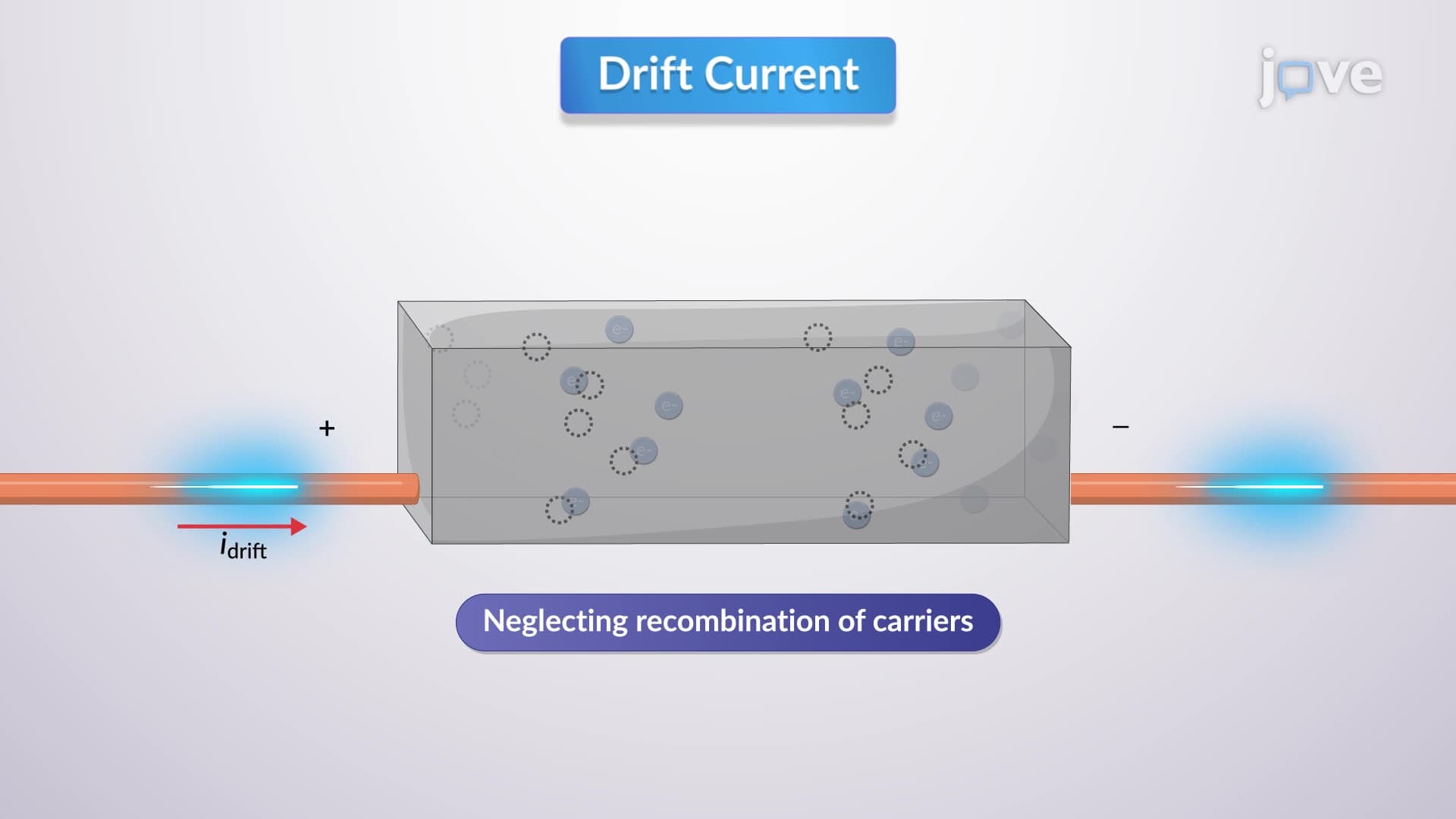
Drift current occurs when an external electric field accelerates charge carriers between atomic collisions. When you apply voltage across a semiconductor device, electrons gain additional velocity beyond their random thermal motion, this extra velocity is called drift velocity. The process resembles how wind pushes leaves in a preferred direction while they still flutter randomly.
The drift velocity depends on carrier mobility, which measures how easily electrons and holes move through the crystal lattice. Higher mobility means carriers respond more readily to electric fields. For silicon at room temperature, electron mobility typically reaches 1350 cm²/(V·s), while hole mobility is lower at 480 cm²/(V·s). This difference explains why n-type semiconductors generally conduct better than p-type materials.
Engineers calculate drift current density using: J(drift) = q × n × μ × E, where q represents elementary charge, n is carrier concentration, μ is mobility, and E is electric field strength. The total conductivity equals the sum of electron and hole contributions, making this relationship crucial for designing efficient transistors and diodes.
Diffusion Current: Concentration-Driven Flow
Diffusion current results from carriers moving randomly from high-concentration regions to low-concentration areas, similar to how perfume molecules spread throughout a room. This process occurs even without applied electric fields, driven purely by thermal energy and concentration gradients.
The diffusion coefficient quantifies how quickly carriers spread due to concentration differences. The Einstein relation connects diffusion coefficient (D) to mobility (μ): D/μ = kT/q, where k is Boltzmann's constant and T is absolute temperature. This relationship proves essential for MCAT physics problems and AP Physics courses covering semiconductor behavior.
Practical Applications in US Technology
Major US semiconductor companies like Intel and AMD rely on precise carrier transport control when manufacturing computer processors. In solar panels across Texas and Arizona, photons create electron-hole pairs that separate through combined drift and diffusion, generating the photocurrent that powers homes and businesses. Understanding these principles helps students excel in engineering programs at institutions like MIT, Stanford, and UC Berkeley.
Frequently Asked Questions
Carrier transport describes how electrons and holes move through semiconductors to create electrical current through drift and diffusion mechanisms. This fundamental process enables all electronic devices to function, from smartphones to solar panels. Understanding carrier transport is essential for physics students and future engineers working in America's $500 billion semiconductor industry.
A p n junction forms where p-type and n-type semiconductor regions meet, creating a boundary where carrier transport becomes crucial for device operation. Carrier transport mechanisms, both drift under electric fields and diffusion across concentration gradients, determine how current flows through the junction. This relationship underlies diode and transistor behavior in electronic circuits.
MCAT Physical Sciences sections frequently test drift velocity calculations and Einstein relation problems involving carrier transport in biological sensors. AP Physics C exams include questions about electric field effects on charge carriers and conductivity calculations. Students should practice relating mobility, electric field strength, and current density using fundamental transport equations.
Silicon Valley's computer processors rely on controlled carrier transport in billions of transistors to process information at gigahertz speeds. California's solar farms generate electricity when photons create electron-hole pairs that separate through transport mechanisms. LED streetlights across American cities work because carrier transport allows electrons and holes to recombine and emit light efficiently.
Basic carrier transport requires only algebra and simple physics concepts taught in high school courses. While advanced semiconductor engineering involves calculus and differential equations, introductory understanding focuses on proportional relationships between mobility, electric fields, and current density. Most students can master fundamental principles with consistent practice and visual aids.
Create concept maps connecting drift current, diffusion current, and total current relationships while practicing numerical problems involving mobility and electric field calculations. Focus on understanding physical meanings behind equations rather than memorizing formulas. Work through practice problems from previous AP Physics or college midterm exams to build confidence with quantitative applications.
Build on carrier transport knowledge by exploring p n junction behavior, diode characteristics, and transistor operation in electronic devices. Advanced students should investigate band theory, doping mechanisms, and semiconductor device physics. These concepts prepare students for electrical engineering programs and careers in America's growing renewable energy and electronics industries.
Related Micro-courses