Loading subject page…

- Electrical Engineering
- Transistors
- Characteristics of JFET
Micro-course: Transistors
16,906 views
Learn key concepts and earn your certificate.

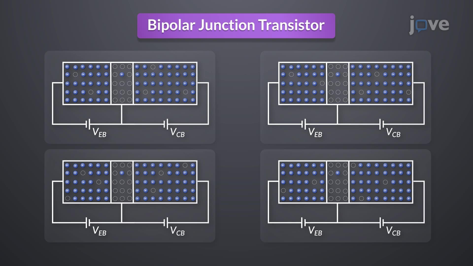
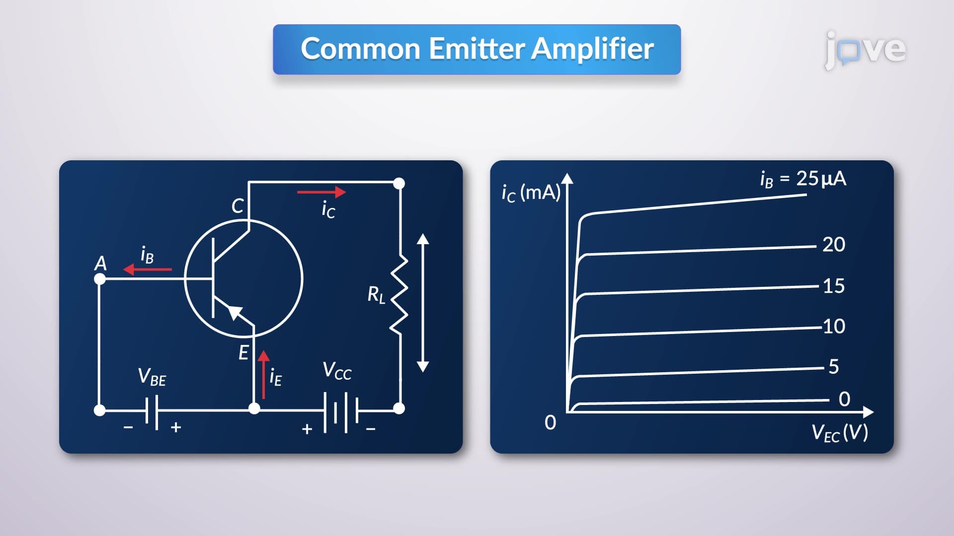
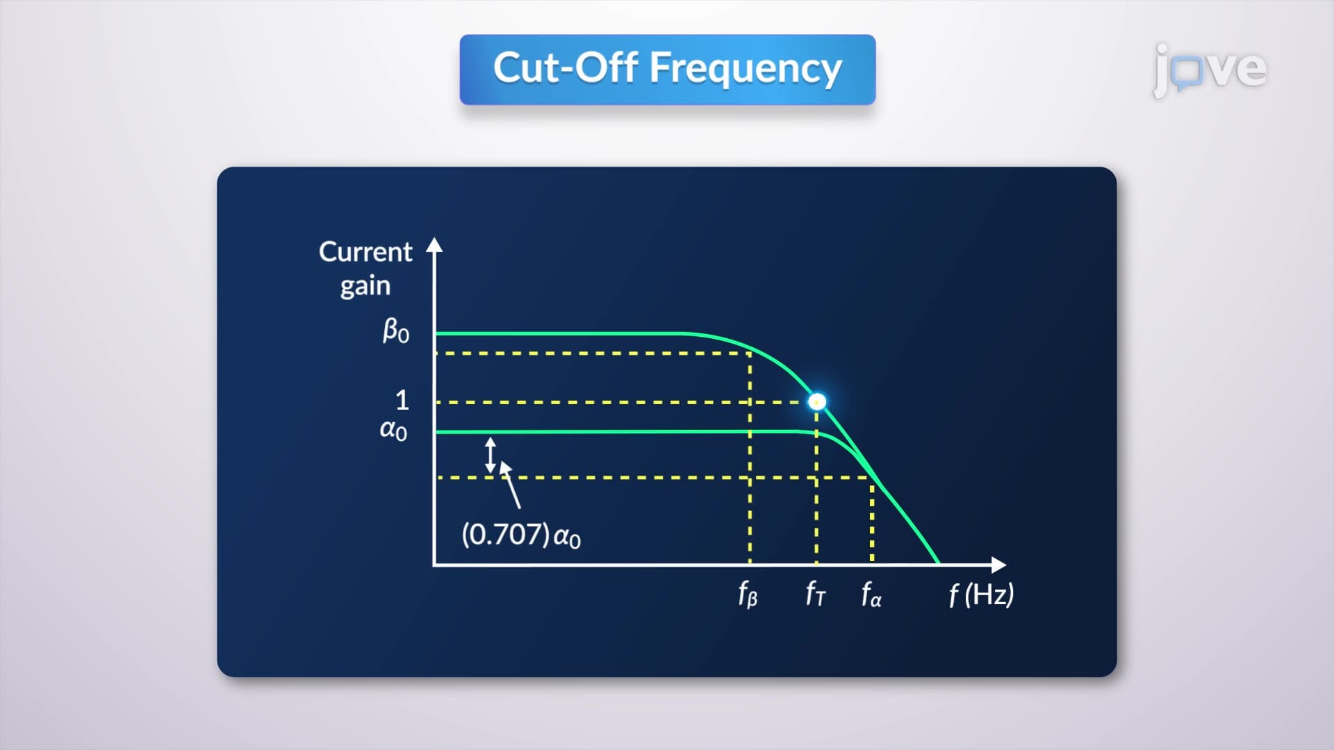
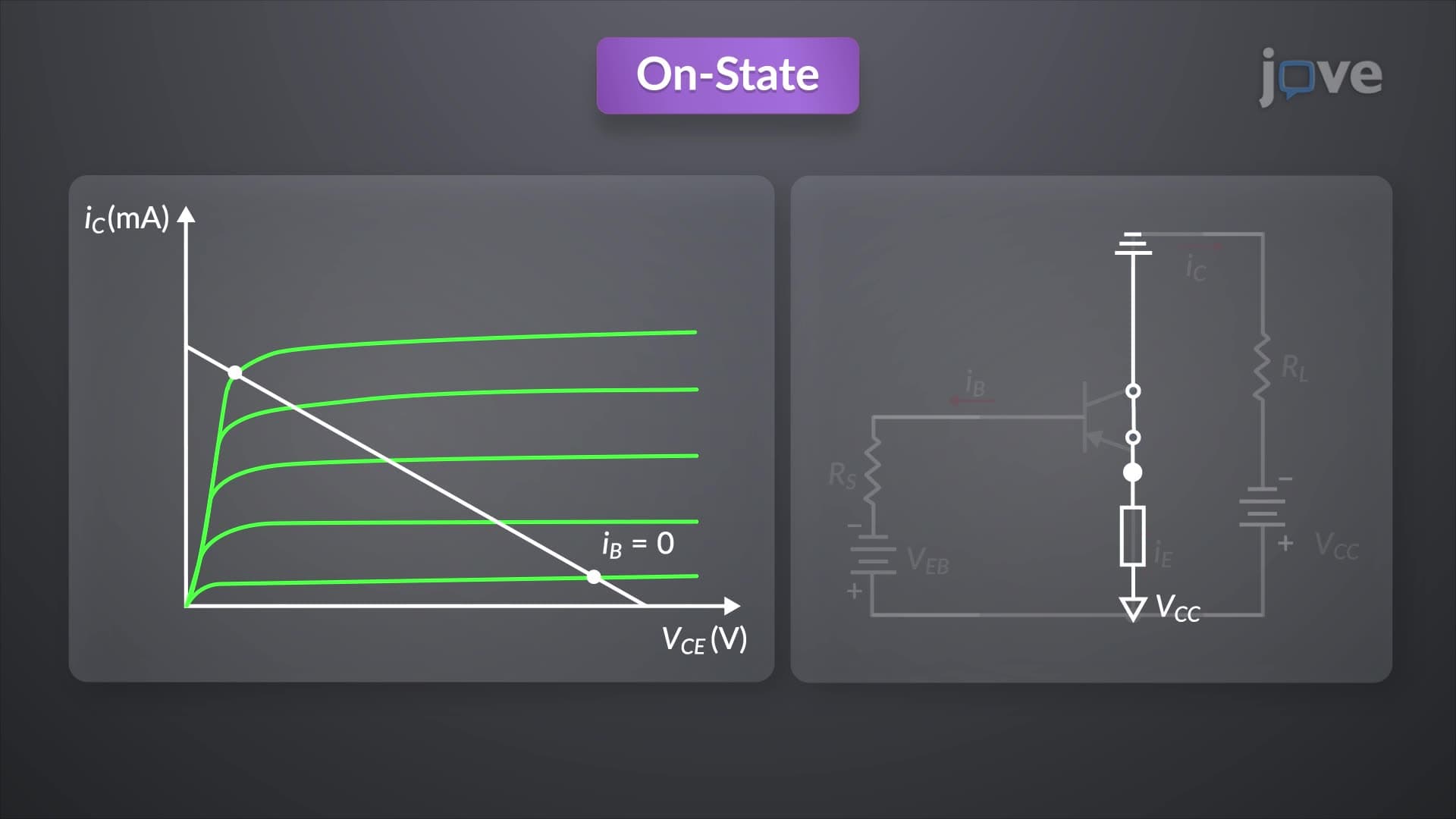
Characteristics of JFET

00:00
01:21
Video Summary: What are Characteristics of Jfet
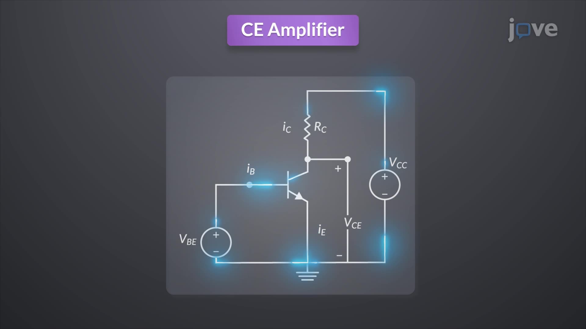
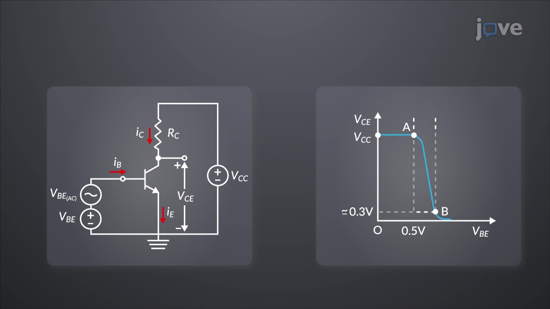
Every smartphone amplifier relies on precisely controlled current flow-but how do engineers achieve this level of control? The biasing of FET devices, particularly understanding what are characteristics of JFET, forms the foundation of modern electronics from Texas Instruments' audio processors to Intel's memory circuits. JFETs operate through three distinct regions: the linear region where they act as voltage-controlled resistors, the saturation region ideal for amplification, and the dangerous breakdown region that can destroy the device. Watch the full video on JoVE Coach to master this concept with expert-led visuals and step-by-step explanations.
- Understand what are characteristics of JFET and how these properties determine device behavior in electronic circuits
- Identify the three operational regions of JFETs: ohmic/linear, saturation/pinch-off, and breakdown regions
- Analyze the relationship between drain current, drain-source voltage, and gate-source voltage in JFET operation
- Compare JFET behavior as a voltage-controlled resistor versus an amplifier based on operating region
- Evaluate the role of depletion layer expansion in controlling current flow through the channel
- Apply JFET characteristics to determine appropriate biasing conditions for specific circuit applications
- Recognize how pinch-off voltage affects the transition between linear and saturation regions
- Explore the practical implications of JFET breakdown voltage in circuit design and safety considerations
Understanding What are Characteristics of JFET
Junction Field-Effect Transistors (JFETs) represent fundamental building blocks in analog electronics, with their characteristics defining how these devices control current flow. The biasing of FET devices requires thorough understanding of how JFETs respond to different voltage conditions, making this knowledge essential for students preparing for AP Physics, college electronics courses, and engineering programs.
The Three Operational Regions of JFETs
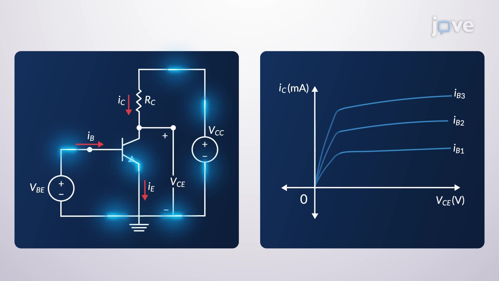
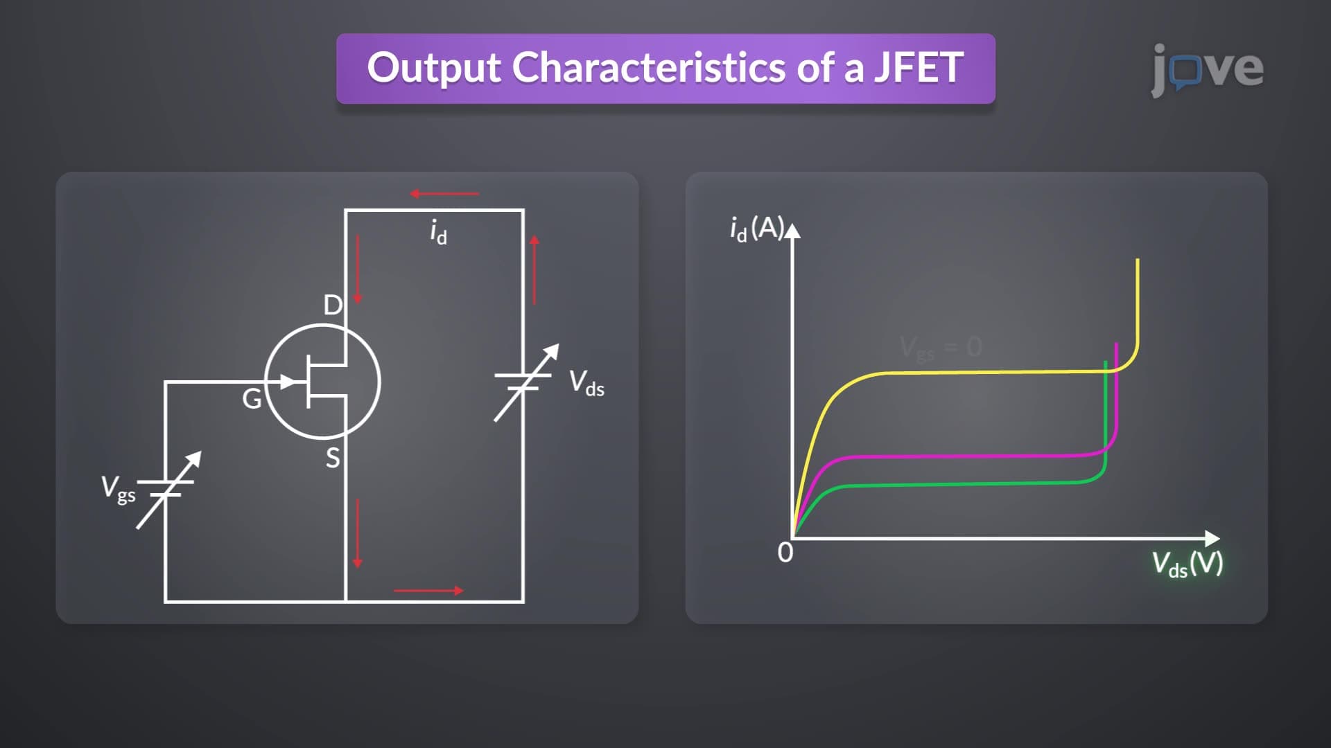
The biasing of FET definition encompasses understanding how JFETs operate across three distinct regions. In the ohmic or linear region, the device functions as a voltage-controlled resistor. Here, small changes in gate voltage produce proportional changes in channel resistance, making this region ideal for electronic switching applications found in automotive control systems and industrial automation.
As drain-source voltage increases, the JFET enters the saturation or pinch-off region. This transition occurs when depletion regions from the gate-channel junctions meet, creating a "pinch-off" effect that limits current flow. Major semiconductor companies like Analog Devices and Linear Technology design amplifier circuits specifically to operate JFETs in this region, where current remains relatively constant despite voltage changes.
Biasing Fundamentals and Practical Applications
What is biasing of FET in detail involves establishing proper operating points within these characteristic regions. Engineers at companies like Boeing and General Electric use sophisticated biasing networks to ensure JFETs operate reliably across temperature variations and component tolerances. The biasing of FET concept requires calculating resistor values that establish appropriate gate-source voltages while considering the device's transconductance and output resistance.
Students encountering this material in college electronics courses should focus on the mathematical relationships governing JFET behavior. The square-law relationship between drain current and gate-source voltage becomes particularly important for MCAT physics sections and engineering program entrance exams.
Critical Design Considerations
The breakdown region represents a destructive operating mode where excessive drain-source voltage causes avalanche multiplication, potentially destroying the device permanently. Understanding this limitation proves crucial for circuit designers at NASA's Jet Propulsion Laboratory and other high-reliability applications where component failure carries significant consequences.
Modern JFET applications span from precision instrumentation at companies like Keysight Technologies to high-frequency communications systems developed by Raytheon and Lockheed Martin, demonstrating the enduring relevance of mastering JFET characteristics.
Frequently Asked Questions
JFET characteristics describe how drain current varies with drain-source voltage across different gate-source voltage levels. These characteristics determine whether the device functions as a resistor, amplifier, or switch. Understanding these relationships is fundamental for designing electronic circuits and appears frequently on AP Physics exams and college electronics courses.
MCAT physics sections often test JFET biasing through circuit analysis problems requiring students to identify operating regions. AP Physics C exams may include questions about current-voltage relationships and the role of electric fields in depletion layer formation. College midterms typically focus on calculating bias resistor values and predicting circuit behavior.
College electronics exams require algebra skills for Ohm's law calculations and basic calculus for understanding transconductance. Students should be comfortable with exponential relationships and graphical analysis of current-voltage characteristics. Most problems involve substituting values into standard biasing equations rather than complex mathematical derivations.
Texas Instruments uses JFETs in precision analog circuits for medical devices, while Intel incorporates them in memory interface circuits. Audio equipment manufacturers like Fender use JFETs in guitar amplifiers for their low-noise characteristics. NASA employs JFETs in satellite communication systems due to their radiation tolerance and reliability.
High school students can absolutely master JFET biasing concepts with proper foundation in basic electronics. The key is starting with simple voltage divider circuits before progressing to active biasing methods. Many students successfully learn this material in AP Physics C or dual-enrollment college courses, making it accessible with dedicated practice.
Focus on drawing and interpreting characteristic curves, as visual understanding helps with both conceptual questions and numerical problems. Practice identifying operating regions from given voltage values, and work through complete bias circuit analysis problems. Create summary sheets linking mathematical relationships to physical phenomena in the device.
Progress to MOSFET characteristics and biasing, which builds directly on JFET knowledge while introducing additional concepts like threshold voltage and body effect. Advanced topics include small-signal analysis, frequency response, and integrated circuit design principles used in modern semiconductor manufacturing.
JFETs share common principles with MOSFETs and bipolar transistors, particularly regarding biasing requirements and amplifier operation. Understanding JFET pinch-off helps explain MOSFET saturation, while the concept of voltage-controlled current sources applies across all active devices. This foundation proves essential for advanced analog circuit design courses.
Related Micro-courses

11 Concepts

7 Concepts

5 Concepts