Loading subject page…

- Electrical Engineering
- Transistors
- Small-Signal Analysis of MOSFET Amplifiers
Micro-course: Transistors
16,906 views
Learn key concepts and earn your certificate.

Small-Signal Analysis of MOSFET Amplifiers

00:00
01:23
Video Summary: Small Signal Analysis of Mosfet Amplifiers Explained
Ever wondered how your smartphone's amplifier boosts tiny electrical signals without distortion? The signal and system principles governing MOSFET transistors enable this precise amplification through carefully controlled small-signal conditions. In engineering applications like Intel's processor designs, Small Signal Analysis of MOSFET Amplifiers Explained reveals how limiting input signal magnitude prevents nonlinear distortion while maintaining linear amplification. This analysis demonstrates transconductance calculations and voltage gain relationships essential for modern electronics. Watch the full video on JoVE Coach to master this concept with expert-led visuals and step-by-step explanations.
- Understand the fundamental principles of Small Signal Analysis of MOSFET Amplifiers Explained and how small-signal conditions prevent nonlinear distortion in transistor circuits
- Identify the three distinct components of instantaneous drain current: DC bias current, signal-proportional component, and nonlinear distortion term
- Analyze how transconductance represents the ratio between output drain current and input gate-source voltage in signal and system applications
- Apply small-signal approximations to neglect higher-order nonlinear terms and achieve linear amplification characteristics
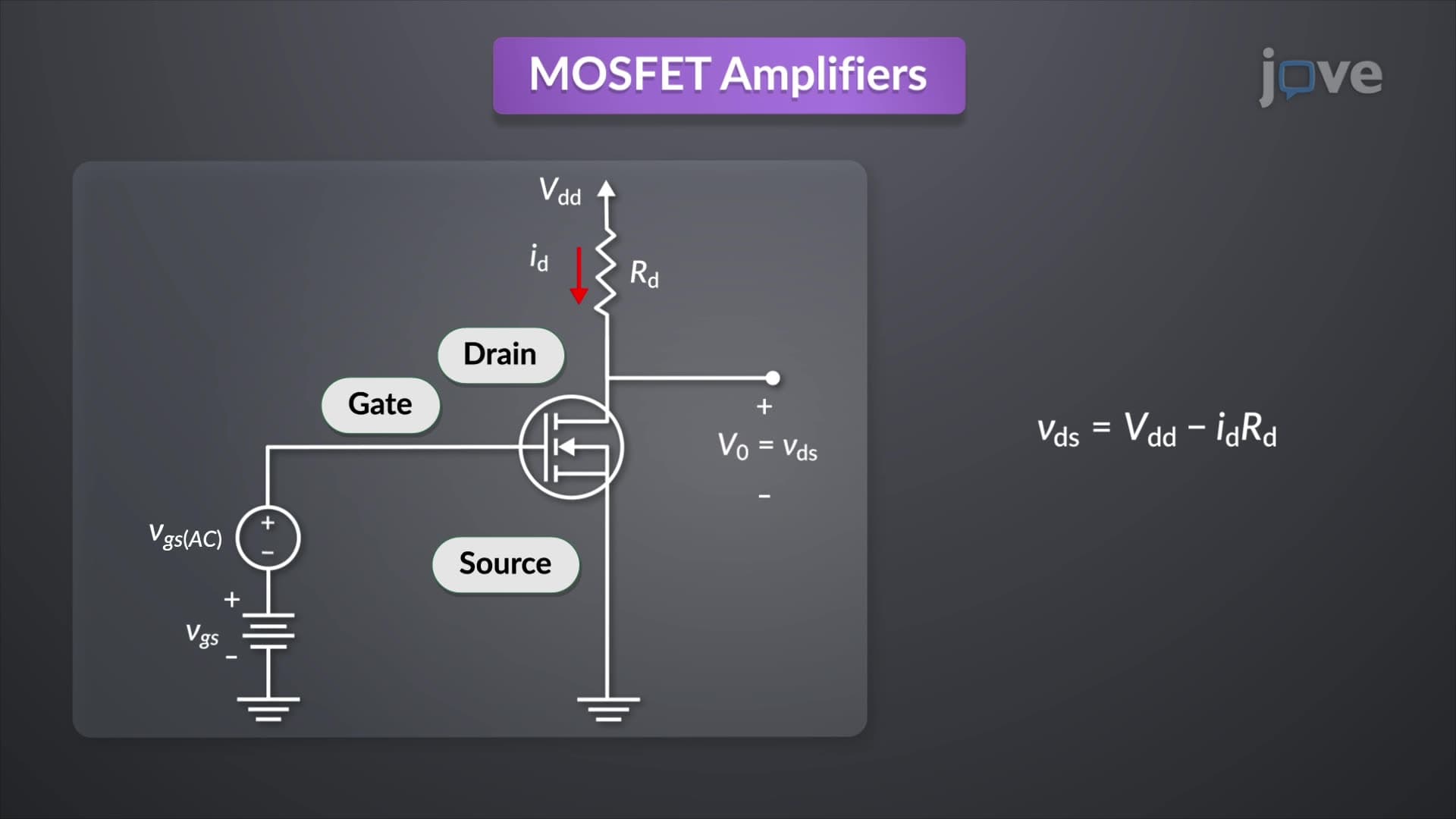
- Evaluate voltage gain calculations using the relationship between transconductance and load resistance in amplifier circuits
- Recognize the 180-degree phase shift indicated by the negative sign in voltage gain expressions
- Compare DC bias conditions with signal components to understand total instantaneous voltage and current relationships
- Explore how characteristic curve slopes at bias points determine transconductance values for practical amplifier design
Understanding Small Signal Analysis of MOSFET Amplifiers
Small signal analysis forms the cornerstone of modern amplifier design, enabling engineers to predict and control electronic circuit behavior with remarkable precision. This analytical approach assumes that input signals remain sufficiently small to maintain linear relationships between input and output parameters. In signal and system theory, this linearity principle allows complex circuit analysis through simplified mathematical models.
MOSFET Operating Regions and Bias Conditions
MOSFET transistors operate in three distinct regions: cutoff, triode, and saturation (active region). For amplification purposes, the transistor must remain in the active region where the relationship between gate-source voltage and drain current exhibits predictable characteristics. The signal and system definition encompasses how DC bias voltages establish the operating point while AC signals create variations around this steady-state condition.
Consider Texas Instruments' operational amplifier designs used in audio equipment. Engineers establish proper bias conditions to ensure the transistor operates in its linear region, preventing signal clipping that would cause audible distortion. The total gate-source voltage combines DC bias (typically 2-5 volts) with the AC input signal (usually millivolts to maintain small-signal conditions).
Transconductance and Signal Relationships
Transconductance (gm) represents the fundamental parameter linking input voltage changes to output current variations. Mathematically expressed as the derivative of drain current with respect to gate-source voltage at the bias point, transconductance determines amplifier sensitivity and gain characteristics. What is signal and system in detail becomes clearer when examining how this parameter enables precise signal processing in applications from smartphone amplifiers to medical device instrumentation.
For AP Physics students preparing for college-level electronics courses, understanding transconductance provides essential foundation knowledge. The parameter typically ranges from 1-100 millisiemens in common MOSFET devices, directly influencing achievable voltage gains in practical circuits.
Voltage Gain and Phase Relationships
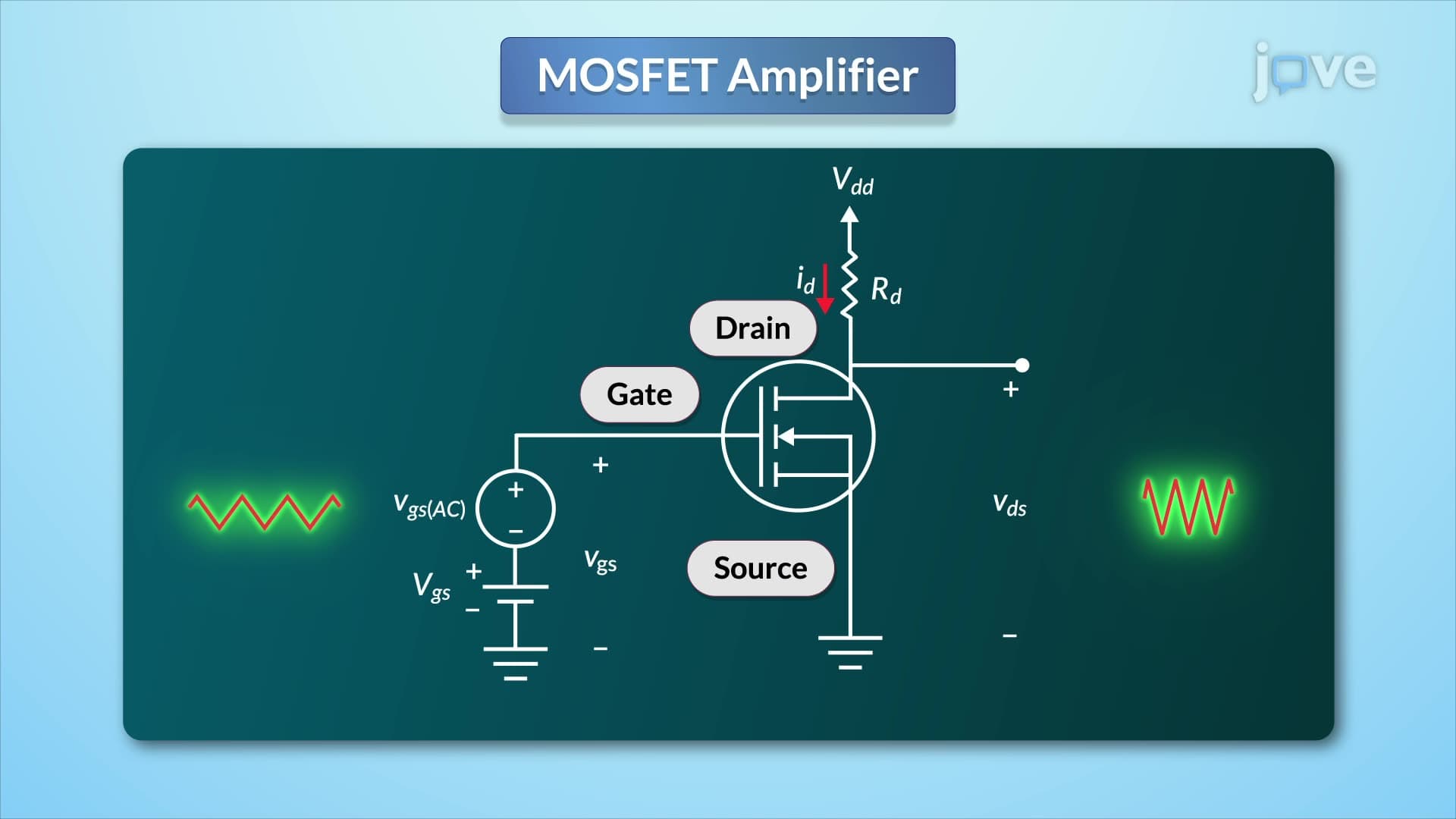
The voltage gain equation (Av = -gm × RL) reveals two critical aspects of MOSFET amplifier behavior. The magnitude determines amplification strength, while the negative sign indicates signal inversion between input and output. This 180-degree phase shift proves crucial in feedback system design and multi-stage amplifier configurations.
Analog Devices and Linear Technology leverage these principles in their precision amplifier products used throughout US industrial and medical applications. Students preparing for the MCAT's physics section encounter similar concepts when studying neural signal processing and biomedical instrumentation systems.
Frequently Asked Questions
Small signal analysis is a method for analyzing MOSFET amplifiers under conditions where input signals remain small enough to maintain linear behavior. This approach prevents nonlinear distortion while enabling predictable amplification characteristics essential for high-quality audio systems, medical devices, and communication equipment. Engineers use this technique to design reliable amplifier circuits with consistent performance specifications.
In signal and system theory, small signal analysis represents a linearization technique that simplifies complex nonlinear relationships into manageable mathematical models. This approach allows engineers to apply superposition principles and frequency domain analysis techniques. The method transforms nonlinear transistor characteristics into linear equivalent circuits, enabling systematic design and analysis procedures used throughout the electronics industry.
Focus on Ohm's law, basic circuit analysis, and voltage-current relationships in resistive networks. Review derivatives and slopes from calculus, as transconductance represents the derivative of current with respect to voltage. Practice calculating voltage gains and understanding phase relationships, as these concepts frequently appear in AP Physics C: Electricity and Magnetism free-response questions.
MCAT passages often present amplifier circuits in biological contexts, such as ECG signal processing or neural recording systems. Questions typically focus on calculating voltage gains, determining output signal characteristics, and analyzing how circuit modifications affect performance. Practice interpreting characteristic curves and relating transconductance values to biological signal amplification requirements found in medical instrumentation.
Electronics courses (EE 101/102), Circuit Analysis (EE 201), and Analog Circuit Design (EE 301) extensively use small signal analysis techniques. These courses appear in electrical engineering, biomedical engineering, and physics degree programs at universities like MIT, Stanford, and UC Berkeley. The concepts also support advanced topics in communication systems and control theory.
Major applications include smartphone audio amplifiers (Apple, Samsung), medical device instrumentation (Medtronic, Boston Scientific), automotive sensor systems (General Motors, Ford), and aerospace electronics (Boeing, Lockheed Martin). These industries rely on precise amplification without distortion for safety-critical applications and high-performance consumer products manufactured across US facilities.
Students with basic algebra and introductory calculus can successfully learn small signal analysis concepts. The mathematical requirements focus on understanding slopes, ratios, and simple derivatives rather than complex mathematical operations. Most concepts build logically from fundamental circuit analysis principles taught in high school physics courses.
Practice drawing equivalent circuits and calculating transconductance from characteristic curves. Work through numerical problems involving voltage gain calculations and phase relationships. Create summary sheets linking mathematical expressions to physical meanings, and solve practice problems from textbooks like Sedra & Smith's "Microelectronic Circuits" commonly used in US universities.
Progress to frequency response analysis, multi-stage amplifier design, and feedback systems theory. Advanced courses cover operational amplifier applications, filter design, and integrated circuit analysis. These topics prepare students for specialized fields like RF engineering, analog IC design, and biomedical instrumentation development offered in graduate programs at leading US engineering schools.
Related Micro-courses

11 Concepts

7 Concepts

5 Concepts